Full-automatic optical detection system for chip detection

A technology of optical detection and chip detection, which is applied in the direction of material analysis, measuring devices, scientific instruments, etc. through optical means, and can solve problems such as inadequacy and low efficiency

Inactive Publication Date: 2019-08-09
中山易美杰智能科技有限公司
View PDF10 Cites 8 Cited by
  • Summary
  • Abstract
  • Description
  • Claims
  • Application Information

AI Technical Summary

Problems solved by technology

[0007] The purpose of the present invention is to provide a fully automatic optical detection system for chip detection, to solve the problems of low efficiency and deficiencies in the prior art caused by manual detection of chips

Method used


Image

  • Full-automatic optical detection system for chip detection
  • Full-automatic optical detection system for chip detection

Examples


Embodiment Construction

[0031] The present invention will be further described below in conjunction with accompanying drawing description and specific embodiment:

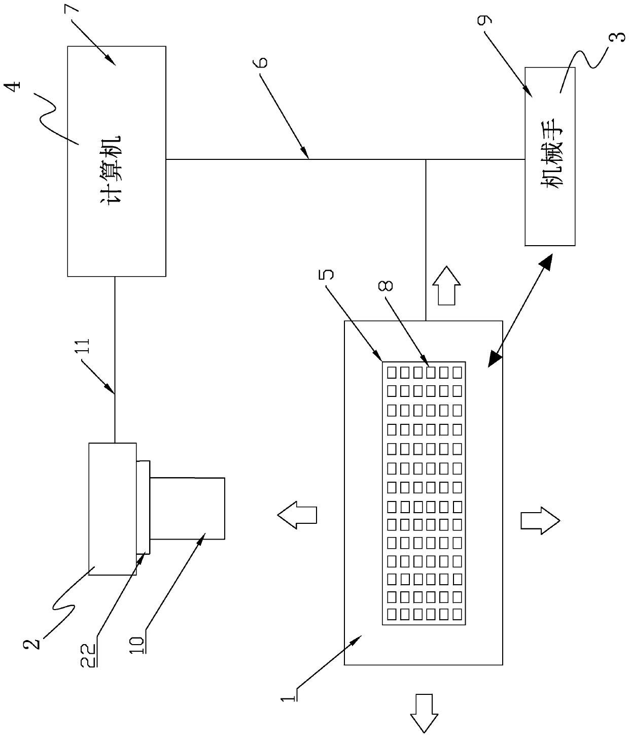
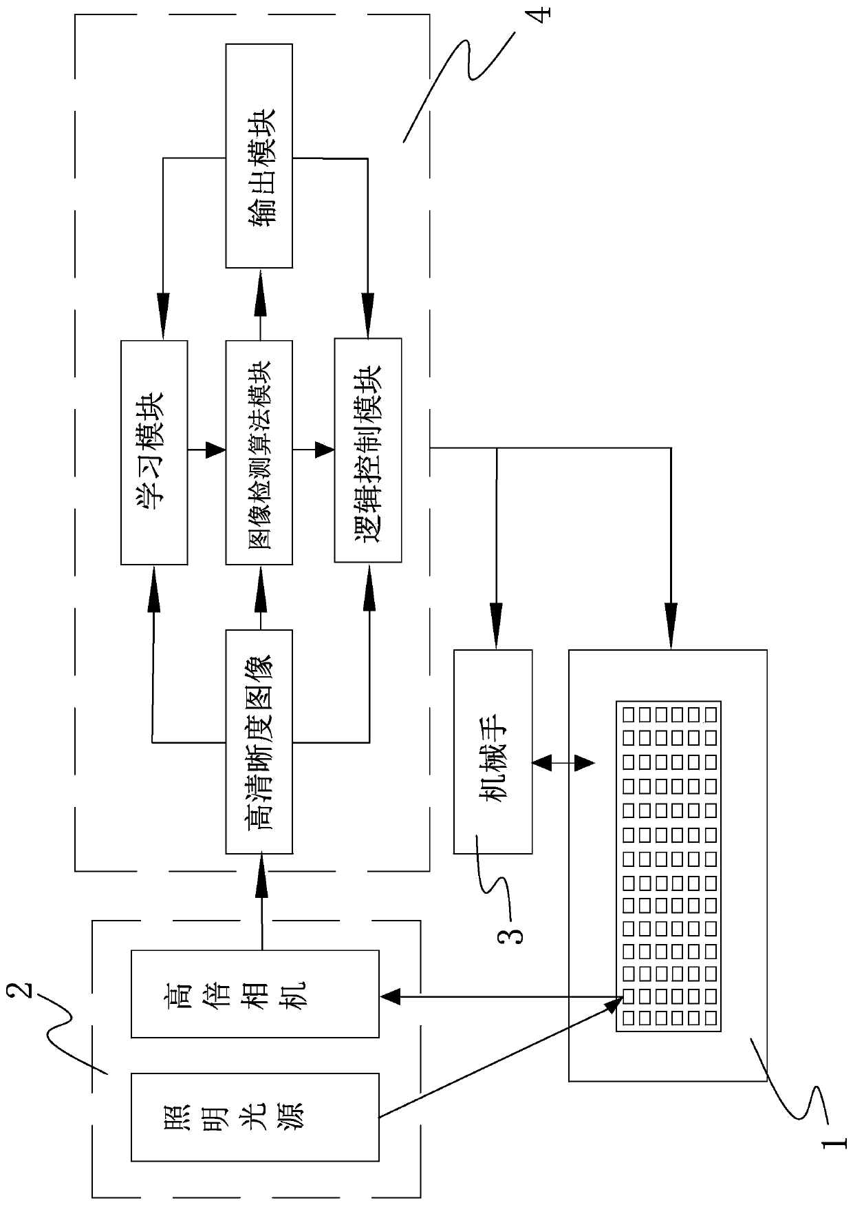
[0032] Such as Figures 1 to 2 A fully automatic optical detection system for chip detection is shown, including:

[0033] The stage 1 is used to place the chip 5 and can move in any direction to realize the path planning of the detection, and accurately and quickly detect each chip 8;

[0034] The loading and unloading device 3 is used to grab the chips to be inspected, place the chips to be inspected on the stage 1 or remove them from the stage 1, the loading and unloading device 3 is arranged on one side of the stage 1, and the The loading and unloading device 3 is a manipulator 9;

[0035] Acquisition device 2 is used to obtain chip image information on the stage 1. The acquisition device 2 is arranged above the object stage 1. The acquisition device 2 is a high-power camera 10. The acquisition device 2 is provided with a device cap...


PUM


Abstract

The invention discloses a full-automatic optical detection system for chip detection. The full-automatic optical detection system for chip detection comprises an objective table, a feeding and discharging device, an acquisition device, a detection system and a logic control module, wherein the acquisition device is controlled to shoot chip image information on the objective table, and whether solder joints of chip gold wires and pins in a chip are qualified or not is analyzed and judged according to the chip image information; and the logic control module is used for controlling the feeding and discharging device to place the chip to be detected on the objective table, the objective table is controlled to move to a shooting area of the acquisition device, and the chip detected on the objective table is taken down. The purpose of the full-automatic optical detection system for chip detection is to provide a method for replacing traditional manual naked eyes to detect the chip, the advanced computer technology and the artificial intelligence technology are adopted, and a manipulator and the objective table are controlled to move according to instructions through the advanced machinelearning software; a product is scanned by a high-power camera to obtain the image information of the solder joints of the chip gold wires and the pins, the quality of the solder joints is judged, andfull-automatic detection is achieved.

Description

technical field [0001] The invention relates to a fully automatic optical detection system for chip detection. Background technique [0002] The chip is the carrier of the integrated circuit. The production process of the integrated circuit chip is from the design of the chip company to the production of the chip foundry to the packaging and testing of the packaging and testing factory, and finally purchased by the complete machine manufacturer. In this process, the packaging and testing stage of the packaging and testing factory determines the output of chips, which affects product benefits. Therefore, an efficient chip detection method is particularly important, and the traditional chip detection industry is a labor-intensive industry. At present, chip inspection mainly relies on manually inspecting the welding quality of each gold wire and its solder joints at both ends under a microscope with the naked eye. Traditional manual inspection requires a lot of manpower and ma...

Claims


Application Information

Patent Timeline
Patent Type & Authority Applications(China)
IPC IPC(8): G01N21/956
CPCG01N21/956
Inventor 苑杰徐维超彭斌田小丰冯永生张琦
Owner 中山易美杰智能科技有限公司
Why Eureka
Try Eureka