Display panel and display device
A technology for display panels and display areas, which is applied in the manufacturing of electrical components, electrical solid-state devices, semiconductor/solid-state devices, etc., can solve the problems of inability to achieve ultra-narrow borders, prone to cracks, affecting display performance, etc., to improve packaging quality and Display performance, prolong life effect
- Summary
- Abstract
- Description
- Claims
- Application Information
AI Technical Summary
Problems solved by technology
Method used
Image
Examples
Embodiment Construction
[0028] In order to enable those skilled in the art to better understand the technical solution of the present invention, a display panel and a display device of the present invention will be further described in detail below with reference to the drawings and specific embodiments.
[0029] The terms "first", "second", "third", etc. (if any) in the description and claims of the present invention and the above drawings are used to distinguish similar objects and not necessarily to describe a specific order or sequentially. It should be understood that the items so described are interchangeable under appropriate circumstances. Furthermore, the terms "comprising" and "having", as well as any variations thereof, are intended to cover a non-exclusive inclusion.
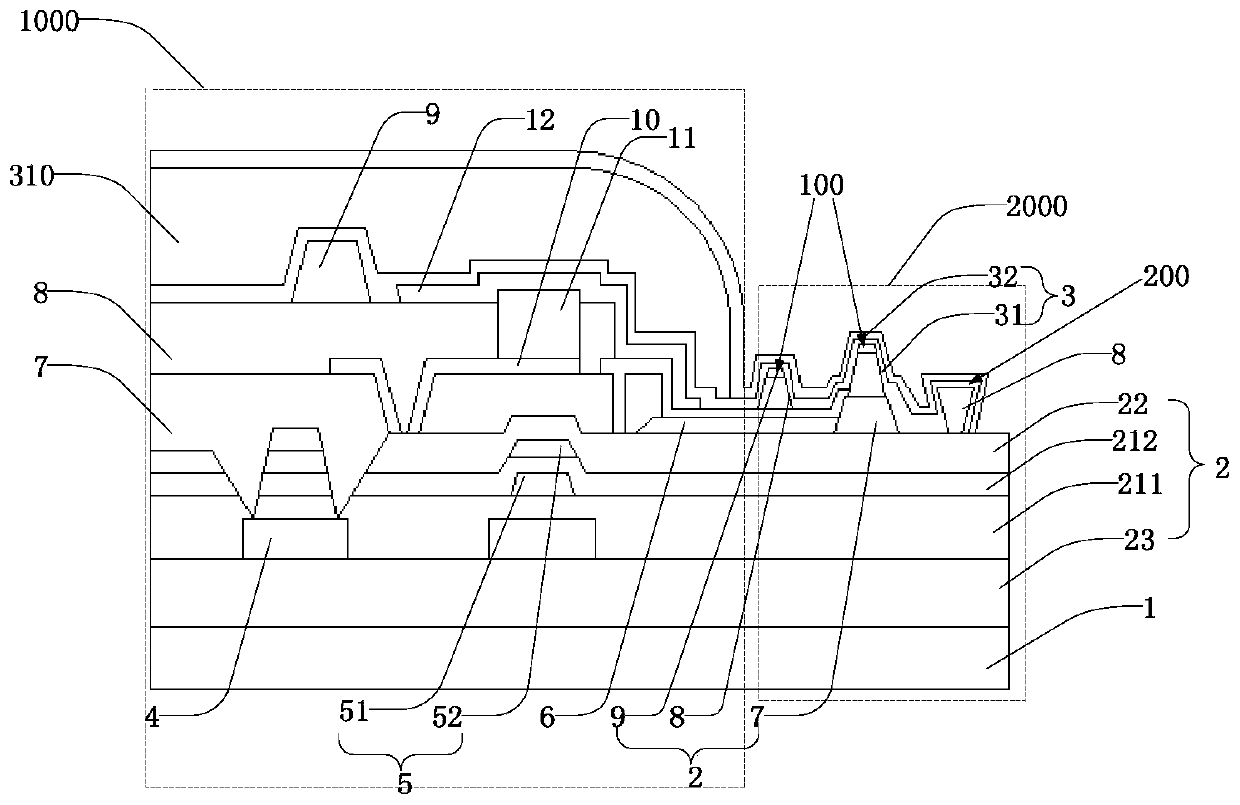
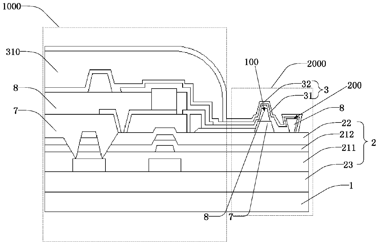
[0030] Such as Figure 1~2 As shown, this embodiment provides a display panel, including a display area 1000 and a non-display area 2000 , the non-display area 2000 surrounds the display area 1000 , and a substrate 1 with...
PUM
 Abstract
Description
Claims
Application Information

