OLED display panel and display device having the same
A technology for display panels and non-display areas, applied in identification devices, static indicators, organic semiconductor devices, etc., can solve problems such as easy cracks, water and oxygen intrusion, and shorten the service life of OLED display panels, so as to prevent cracks and ensure The effect of improving the service life and package reliability
- Summary
- Abstract
- Description
- Claims
- Application Information
AI Technical Summary
Problems solved by technology
Method used
Image
Examples
Embodiment 1
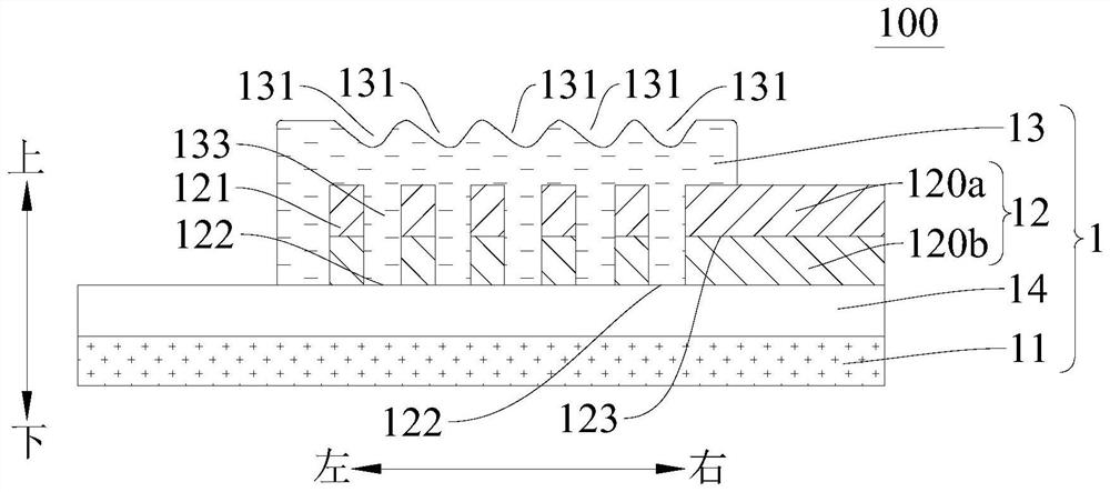
[0073] In this embodiment, as figure 1 As shown, the OLED display panel 100 has a non-display area, and the non-display area includes an encapsulation part encapsulated by the encapsulation layer and an edge part 1 that is not encapsulated by the encapsulation layer. The edge part 1 includes a flexible substrate 11, a buffer layer 14, Inorganic layer 12 and organic layer 13 .
[0074] The buffer layer 14 is provided on the upper surface of the upper flexible substrate 11 , the inorganic layer 12 is provided on the upper surface of the buffer layer 14 , and the inorganic layer 12 includes an inorganic layer body 123 , 5 dams 121 and 5 grooves 122 , 5 dams 121 and 5 grooves 122 are located at the edge of the inorganic layer 12, and the 5 dams 121 and the 5 grooves 122 are alternately arranged from outside to inside, and a groove 122, A dam portion 121 is formed between two adjacent groove portions 122 , and a groove portion 122 is defined between the innermost one of the five d...
Embodiment 2
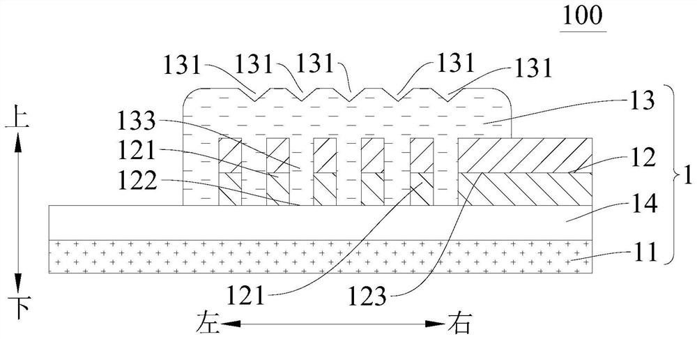
[0080] like figure 2 As shown, the structure of this embodiment is substantially the same as that of the first embodiment, wherein the same components are given the same reference numerals, the difference is that the cross-sectional width of each stress groove 131 decreases linearly from top to bottom, and each stress groove 131 decreases linearly from top to bottom. The bottom surface of each stress slot 131 is a combination of two intersecting planes, so that the stress slot 131 is roughly formed as a V-shaped slot.
Embodiment 3
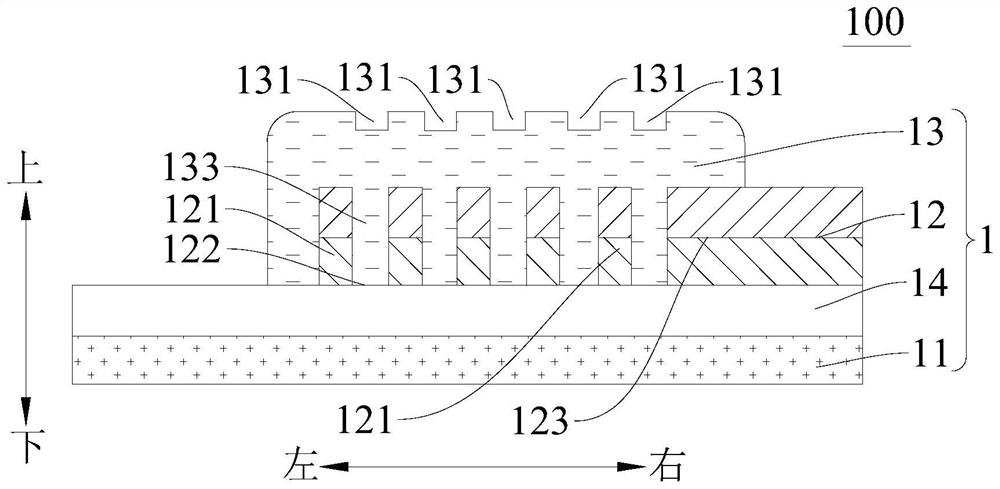
[0082] like image 3 As shown, the structure of this embodiment is substantially the same as that of the first embodiment, wherein the same components are given the same reference numerals, the difference is that the cross-sectional width of each stress groove 131 remains unchanged from top to bottom, and each The bottom surface of the stress groove 131 is flat.
PUM
 Abstract
Description
Claims
Application Information
 - R&D
- Intellectual Property
- Life Sciences
- Materials
- Tech Scout
- Unparalleled Data Quality
- Higher Quality Content
- 60% Fewer Hallucinations
Browse by: Latest US Patents, China's latest patents, Technical Efficacy Thesaurus, Application Domain, Technology Topic, Popular Technical Reports.
© 2025 PatSnap. All rights reserved.Legal|Privacy policy|Modern Slavery Act Transparency Statement|Sitemap|About US| Contact US: help@patsnap.com


