
Latch register

A latch and inverter technology, applied in the field of latches, can solve problems such as false inversion of logic states

Active Publication Date: 2019-08-16
SHANGHAI HUALI MICROELECTRONICS CORP
View PDF4 Cites 0 Cited by
  • Summary
  • Abstract
  • Description
  • Claims
  • Application Information

AI Technical Summary

Problems solved by technology

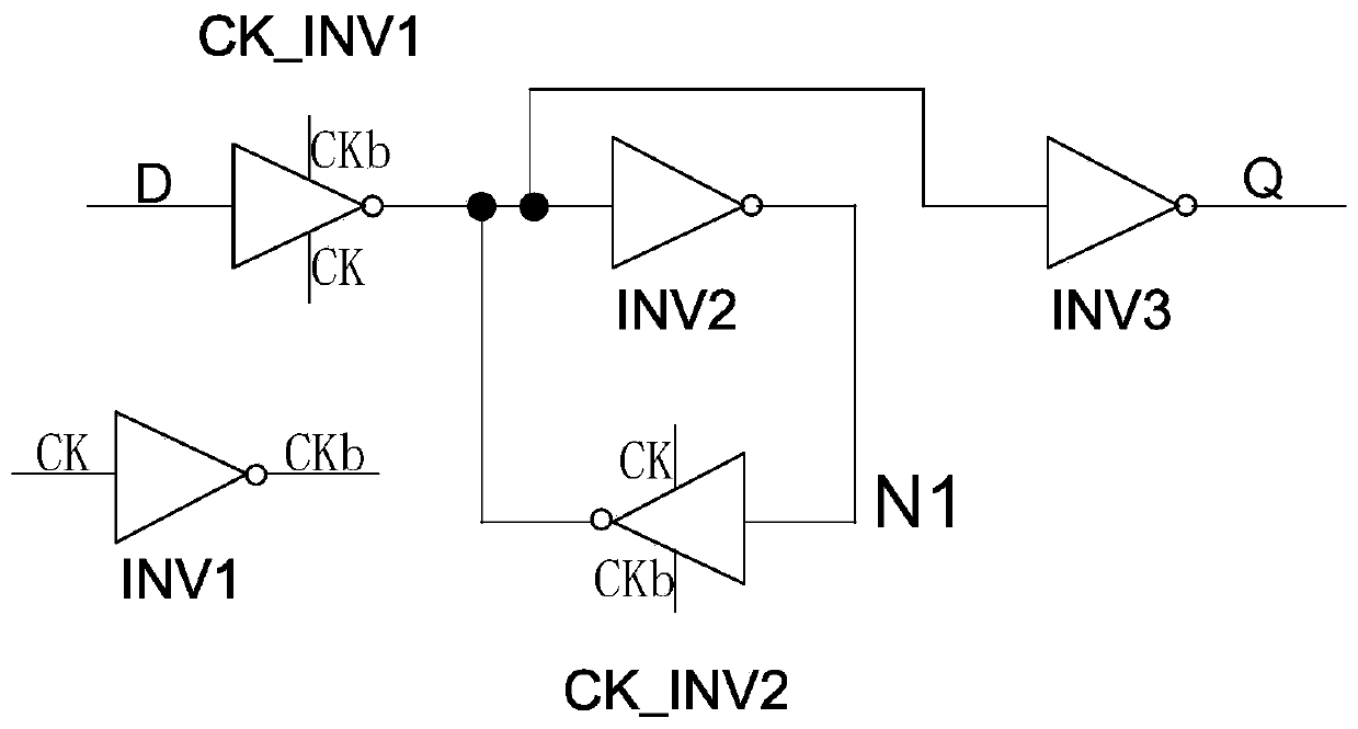
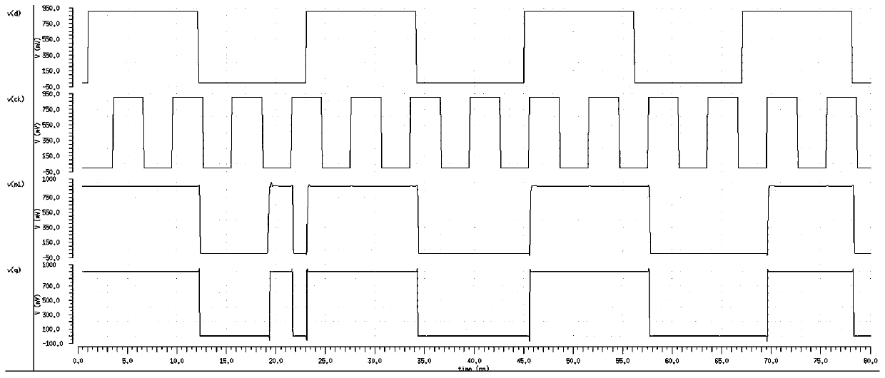
For this type of latch, when the latch signal is output, if the latch circuit (N1 node) is disturbed by signals such as noise, the logic state of the latch may be changed, so that the logic state of the output is wrongly reversed.

Method used


Image

  • Latch register
  • Latch register
  • Latch register

Examples


Embodiment Construction

[0065] Embodiments of the present invention are described below through specific examples, and those skilled in the art can fully understand other advantages and technical effects of the present invention from the content disclosed in this specification. The present invention can also be implemented or applied through different specific implementation modes, and various details in this specification can also be applied based on different viewpoints, and various modifications or changes can be made without departing from the general design idea of ​​the invention. It should be noted that, in the case of no conflict, the following embodiments and features in the embodiments can be combined with each other.

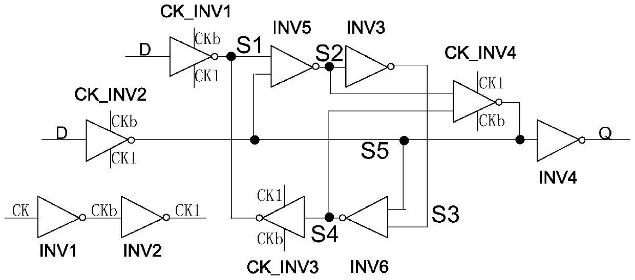
[0066] refer to figure 2 As shown, a feasible embodiment of the latch provided by the present invention includes first to fourth clocked inverters CK_INV1 to CK_INV4 and first to sixth inverters INV1 to INV6;

[0067] The first inverter INV1, the input end of which is conn...


PUM


Abstract

The invention discloses a latch register. An input end of a first inverter is connected with a clock signal; the input end of a second inverter is connected with the output end of the first inverter;the input ends of the first and second clock control inverters are connected with a latch input signal D and the output ends of the first and second inverters; the input end of the fourth inverter isconnected with the output ends of the second clock control inverter and the fourth clock control inverter, the output end of the fourth inverter serves as the output end of the latch, the input end ofthe fifth inverter is connected with the output ends of the first clock control inverter, the second clock control inverter and the third clock control inverter, and the input end of the third inverter is connected with the output end of the fifth inverter; the input end of the sixth inverter is connected with the output ends of the second clock control inverter and the third inverter; the inputend of the third clock control inverter is connected with the output ends of the first, second and sixth inverters; and the input end of the fourth clock control inverter is connected with the outputends of the first, second, fifth and sixth inverters. Compared with the prior art, the latch register has better signal interference resistance and higher reliability.

Description

technical field [0001] The invention relates to the field of integrated circuits, in particular to a latch. Background technique [0002] A latch (Latch) is a type of logic element with a memory function in a digital circuit. Latch is to temporarily store the signal to maintain a certain level state. In digital circuits, binary digital signals "0" and "1" can be recorded. The state of the input is saved to the output only when there is a latch signal until the next latch signal. Usually there are only two values ​​0 and 1. A latch (Latch) is a memory cell circuit that is sensitive to pulse levels, and they can change states under the action of a specific input pulse level. [0003] Such as figure 1 As shown, a traditional latch includes a first inverter INV1, a second inverter INV2, a third inverter INV3, a first clocked inverter CK_INV1 and a second clocked inverter CK_INV2 . The first inverter INV1 inverts the clock signal CK to become CKb. The first clock-controlle...

Claims


Application Information

Patent Timeline
IPC IPC(8): H03K19/003
CPCH03K19/00315Y02D10/00
Inventor 虞蓓蕾高唯欢胡晓明
Owner SHANGHAI HUALI MICROELECTRONICS CORP
Learn More