
Organic light-emitting diode display panel and manufacturing method thereof

A technology of light-emitting diodes and display panels, which is applied in semiconductor/solid-state device manufacturing, electrical components, electric solid-state devices, etc., can solve the problems of display panel voltage drop increase, resistance increase, display panel power consumption increase, etc., to improve light output The effect of reducing the rate and light output rate

Inactive Publication Date: 2019-08-20
WUHAN CHINA STAR OPTOELECTRONICS SEMICON DISPLAY TECH CO LTD
View PDF16 Cites 8 Cited by
  • Summary
  • Abstract
  • Description
  • Claims
  • Application Information

AI Technical Summary

Problems solved by technology

[0005] The present application relates to an organic light emitting diode display panel and its manufacturing method, which is used to solve the problem in the prior art that the cathode thickness of the display panel is too low to increase the resistance, thereby increasing the voltage drop of the display panel, and finally causing the display panel to fail. Increased power consumption or excessive thickness of the cathode reduces the light output rate

Method used


Image

  • Organic light-emitting diode display panel and manufacturing method thereof
  • Organic light-emitting diode display panel and manufacturing method thereof
  • Organic light-emitting diode display panel and manufacturing method thereof

Examples


Embodiment Construction

[0038] The technical solutions in the embodiments of the present application will be clearly and completely described below in conjunction with the drawings in the embodiments of the present application. Apparently, the described embodiments are only some of the embodiments of this application, not all of them. Based on the embodiments in this application, all other embodiments obtained by those skilled in the art without making creative efforts belong to the scope of protection of this application.

[0039] In the description of the present application, it should be understood that the terms "center", "longitudinal", "transverse", "length", "width", "thickness", "upper", "lower", "front", " Orientation indicated by rear, left, right, vertical, horizontal, top, bottom, inside, outside, clockwise, counterclockwise, etc. The positional relationship is based on the orientation or positional relationship shown in the drawings, which is only for the convenience of describing the a...


PUM


Abstract

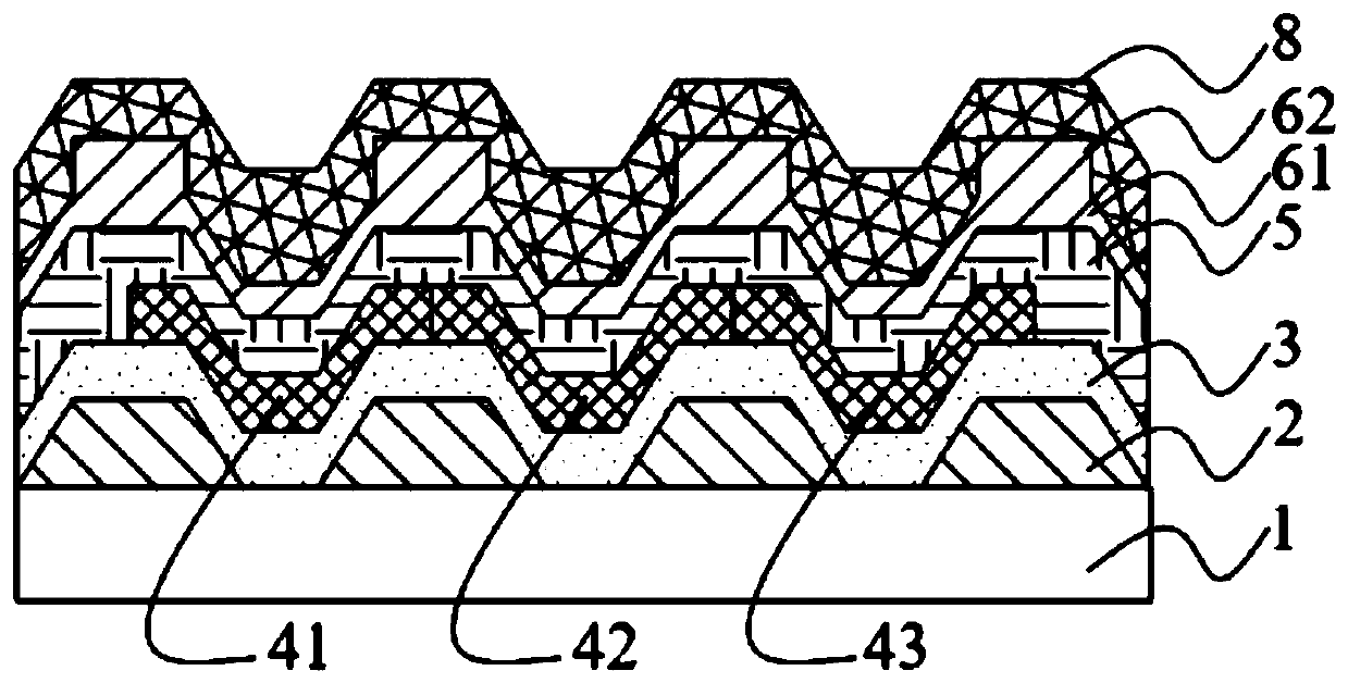
An organic light-emitting diode display panel comprises a substrate, a pixel definition layer, an anode layer, a light-emitting layer, an electron transmission layer, a cathode layer and a reflectionlayer. The cathode layer is arranged on the electron transport layer and has two different thicknesses. The reflection layer is arranged on the cathode layer and is used for improving the light emitting rate. The beneficial effects of the invention are as follows: according to the invention, by adopting a novel evaporation process, the cathode layer in the display panel is divided into a first cathode layer and a second cathode layer; the first cathode layer is arranged right above the pixel layer; the thickness of the first cathode layer is smaller than that of the second cathode layer; the power consumption of the display panel is reduced while the light extraction rate of the organic light-emitting diode display panel is guaranteed; and in addition, the reflection layer is further deposited on the first cathode layer and the second cathode layer, so the light extraction rate is improved.

Description

technical field [0001] The present application relates to the display field, in particular to an organic light emitting diode display panel and a manufacturing method thereof. Background technique [0002] Organic light-emitting devices (organic light-emitting devices, OLEDs) have the advantages of active light emission, low temperature operation, fast light response speed, wide viewing angle, high efficiency, flexible display devices, low driving voltage and low energy consumption, etc. The advantages have attracted the attention of many display manufacturers around the world, and it is considered to be the next generation of display technology. [0003] With the rapid development of new display technologies, OLED displays are endowed with more expectations, such as wider color gamut, higher contrast ratio, lower energy consumption, higher resolution, etc. In the current mainstream panel structure, in order to reduce the absorption of light by the cathode and reduce the lo...

Claims


Application Information

Patent Timeline
Patent Type & Authority Applications(China)
IPC IPC(8): H01L27/32H01L51/52H01L51/56
CPCH10K59/353H10K71/16H10K59/122H10K50/856H10K71/00
Inventor 赵媛媛
Owner WUHAN CHINA STAR OPTOELECTRONICS SEMICON DISPLAY TECH CO LTD
Learn More