A detection method and display device for a chip on a multilayer film and its bonding state

A detection method and multi-layer film technology, applied in measuring devices, circuit inspection/identification, instruments, etc., can solve the problems of increasing the risk of bad bonding products entering the market and increasing hidden dangers of product quality, so as to avoid functional defects, The effect of reducing quality hazards

Active Publication Date: 2021-11-02
BOE TECH GRP CO LTD +1
View PDF0 Cites 0 Cited by
  • Summary
  • Abstract
  • Description
  • Claims
  • Application Information

AI Technical Summary

Problems solved by technology

However, such a chip on a double-layer film cannot use conventional detection methods to detect the bonding state, which increases the risk of bad bonding products entering the market and increases the quality of the product.

Method used


Image

  • A detection method and display device for a chip on a multilayer film and its bonding state
  • A detection method and display device for a chip on a multilayer film and its bonding state
  • A detection method and display device for a chip on a multilayer film and its bonding state

Examples


no. 1 example

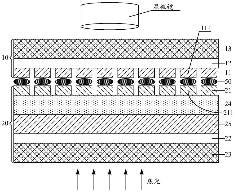
[0067] Figure 4 It is a schematic cross-sectional structure diagram of a chip on a double-layer film according to an embodiment of the present invention, Figure 5 for Figure 4 Schematic diagram of the structure of the middle electrode structure layer. Such as Figure 4 As shown, the double-layer chip-on-film includes a first flexible circuit board 10 and a second flexible circuit board 20 . The first flexible circuit board 10 sequentially includes a first bonding layer 11 , a first adhesive layer 12 and a first protection layer 13 . The second flexible circuit board 20 sequentially includes a second bonding layer 21 , a substrate layer 24 , an electrode structure layer 26 , a second adhesive layer 22 and a second protection layer 23 . The first bonding layer 11 includes a plurality of first connecting ends 111 arranged at intervals in sequence along the first direction, and the second bonding layer 21 includes a plurality of second connecting ends 211 arranged in one-to...

no. 2 example

[0090] Based on the inventive concepts of the foregoing embodiments, the second embodiment of the present invention proposes a method for detecting the bonding state of a chip on a double-layer film. Such as Figure 4 As shown, the double-layer chip-on-film includes a first flexible circuit board 10 and a second flexible circuit board 20 . The first flexible circuit board 10 sequentially includes a first bonding layer 11 , a first adhesive layer 12 and a first protection layer 13 . The second flexible circuit board 20 sequentially includes a second bonding layer 21 , a substrate layer 24 , an electrode structure layer 26 , a second adhesive layer 22 and a second protection layer 23 . The first bonding layer 11 includes a plurality of first connecting ends 111 arranged at intervals in sequence along the first direction, and the second bonding layer 21 includes a plurality of second connecting ends 211 arranged in one-to-one correspondence with the plurality of first connecting...

no. 3 example

[0123] Based on the inventive concepts of the aforementioned embodiments, an embodiment of the present invention further provides a display device, which includes the multilayer chip-on-a-film using the aforementioned embodiments. The display device can be any product or component with a display function such as a mobile phone, a tablet computer, a television, a monitor, a notebook computer, a digital photo frame, a navigator, and the like.


PUM


Abstract

The invention discloses a chip on a multi-layer film, a bonding state detection method thereof, and a display device. The multilayer chip-on-film includes a first flexible circuit board and a second flexible circuit board, the first flexible circuit board includes a plurality of first connection ends, and the second flexible circuit board includes a plurality of second connection ends, so The plurality of first connecting ends are correspondingly bonded to the plurality of second connecting ends, and the second flexible circuit board further includes an electrode structure layer, and the electrode structure layer is used for detecting the connection between the electrode structure layer and the first The capacitance between the connection terminals determines the bonding state of the first connection terminal and the second connection terminal. The multilayer chip-on-film realizes the detection of the bonding state by detecting the capacitance between the electrode structure layer and the first connection end, avoids products with bad bonding from entering the market, and reduces the hidden danger of product quality.

Description

technical field [0001] The invention relates to the field of display technology, in particular to a method for detecting a chip on a multilayer film and its bonding state, and a display device. Background technique [0002] With the development of display technology, display devices sometimes need to use a double-layer chip on film (Chip On Film, COF). The double-layer chip-on-film usually includes a first flexible circuit board with a single-layer structure and a second flexible circuit board with a double-layer structure, and the first flexible circuit board and the second flexible circuit board are connected by bonding. [0003] The combination of the first flexible circuit board and the second flexible circuit board is a combination of soft materials and soft materials. Without the protection of hard materials, it is easy to cause insufficient hardness. Therefore, the non-bonded parts in the second flexible circuit board are usually The bonding metal layer is arranged a...

Claims


Application Information

Patent Timeline
Patent Type & Authority Patents(China)
IPC IPC(8): G01N27/24G01N27/22H05K1/02
CPCG01N27/226G01N27/24H05K1/0268
Inventor 吴昊安娜谢晓波孙兴盼张晓萍郭宝磊蔡斯特次刚马晓曹学文景奇徐斌罗振华郑仰利
Owner BOE TECH GRP CO LTD
Why Eureka
Try Eureka