Display panel and display device

A display panel and display area technology, applied to static indicators, instruments, etc., can solve the problems of increased circuit size of the demultiplexer, increased frame area, and unfavorable design requirements for narrow frame of the display device, etc.

Inactive Publication Date: 2019-08-30
XIAMEN TIANMA MICRO ELECTRONICS
View PDF7 Cites 5 Cited by
  • Summary
  • Abstract
  • Description
  • Claims
  • Application Information

AI Technical Summary

Problems solved by technology

When the number of pixels in the display device further increases, the number of transistors in the demultiplexer circuit increases accordingly, so that the size of the demultiplexer circuit increases, and the occupied frame area increases, which is not conducive to the design requirements of the narrow frame of the display device.

Method used


Image

  • Display panel and display device
  • Display panel and display device
  • Display panel and display device

Examples


Embodiment Construction

[0031] The present invention will be further described in detail below in conjunction with the accompanying drawings and embodiments. It should be understood that the specific embodiments described here are only used to explain the present invention, but not to limit the present invention. In addition, it should be noted that, for the convenience of description, only some structures related to the present invention are shown in the drawings but not all structures.

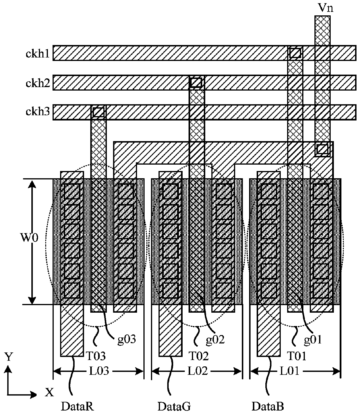
[0032] figure 1 It is a structural schematic diagram of a prior art demultiplexer circuit. Such as figure 1 , the demultiplexer circuit includes three transistors T01, T02 and T03, the input electrodes of the three transistors T01, T02 and T03 are electrically connected with the same data signal pin Vn, the output electrodes of the three transistors T01, T02 and T03 They are respectively electrically connected to different data signal lines DataR, DataG and DataB, and the control electrodes g01, g02 and g03 of t...


PUM


Abstract

The embodiment of the invention provides a display panel and a display device. A plurality of transistors of a multiplexer circuit of the display panel comprise at least one first transistor. The first transistor comprises two control electrodes; the two control electrodes are respectively and electrically connected with the same clock control signal line through different connecting lines; therefore, the length of the first transistor can be increased in the arrangement direction of the data signal lines, the width of the first transistor in the extension direction of the data signal lines isreduced, the occupied area of the multiplexer circuit is reduced, the size of a non-display area in the extension direction of the data signal lines is reduced, and a narrow frame of the display panel is facilitated.

Description

technical field [0001] The present invention relates to the field of display technology, in particular to a display panel and a display device. Background technique [0002] There are multiple pixels in the active matrix display panel, wherein the pixels in the same row can share one scanning signal line, and the pixels in the same column can share one data signal line, and each pixel is provided with a driving transistor, and the scanning signal line can The scanning signal provided by the driving chip is sequentially input to each row of pixels, and the driving transistor of the corresponding pixel is controlled to be turned on. The data signal line can input the data voltage signal provided by the driving chip into the pixel, so that the pixel can display and emit light. [0003] With the development of display technology, the requirements for the display effect of the display panel are getting higher and higher. The number of pixels in the display panel is increasing, an...

Claims


Application Information

Patent Timeline
Patent Type & Authority Applications(China)
IPC IPC(8): G09G3/36G09G3/3225
CPCG09G3/3225G09G3/3648
Inventor 周秀峰周洪波伍黄尧
Owner XIAMEN TIANMA MICRO ELECTRONICS
Why Eureka
Try Eureka