A gate-controlled bipolar-field-effect composite silicon carbide ldmos

A composite silicon carbide and field effect technology, which is applied in the direction of semiconductor devices, electrical components, circuits, etc., can solve the problems of reducing the conduction performance of devices and low electron mobility in MOSFET channels.

Active Publication Date: 2021-04-13
XIDIAN UNIV
View PDF5 Cites 0 Cited by
  • Summary
  • Abstract
  • Description
  • Claims
  • Application Information

AI Technical Summary

Problems solved by technology

However, silicon carbide thermally grown silicon dioxide is not as good as silicon grown, SiC / SiO 2 The interface charge ratio of SiC / SiO 2 about two orders of magnitude higher, especially for SiC-SiO 2 The high interface state density near the conduction band edge at the interface will make the electron mobility of the MOSFET channel relatively low, which will greatly reduce the conduction performance of the device

Method used


Image

  • A gate-controlled bipolar-field-effect composite silicon carbide ldmos
  • A gate-controlled bipolar-field-effect composite silicon carbide ldmos

Examples


Embodiment Construction

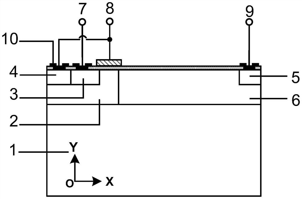
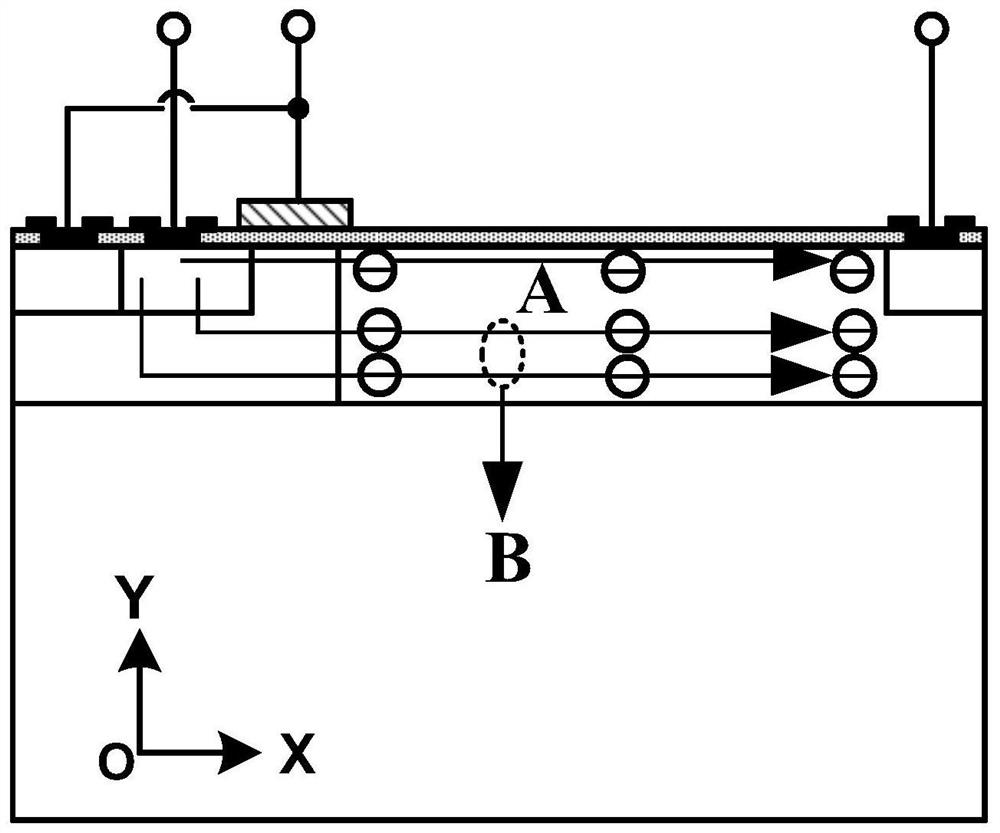
[0029] Such as figure 1 As shown, the gate-controlled bipolar-field-effect composite silicon carbide lateral double-diffused metal-oxide-semiconductor transistor includes:

[0030] Silicon carbide substrate 1, the doping concentration is the concentration of general silicon carbide single crystal material, the typical value is 1×10 18 cm -3 ~1×10 19 cm -3 ;

[0031] growing an epitaxial layer on the substrate;

[0032] forming a base region 2 on the epitaxial layer;

[0033] A drift region 6 is formed on the epitaxial layer; the material of the drift region is silicon carbide, and the doping concentration is 1×10 15 cm -3 ;

[0034] Forming an active region on the surface of the device;

[0035] a gate insulating layer formed on the active region, and forming a gate 8 above the gate insulating layer;

[0036] A source region 3 is formed on the base region in contact with a base region contact 4 and a channel is formed on the base region; wherein, the doping concentra...


PUM


Abstract

The invention discloses a gate-controlled bipolar-field effect composite silicon carbide LDMOS, the substrate of which is made of silicon carbide, the surface in contact with the base forms a base, the base is isolated from the source, and electrically connected to the gate, replacing the traditional In the silicon carbide LDMOS, the electrode connection mode of the base region and the source is short-circuited, satisfying that when the gate is connected to the voltage, the voltage obtained by the base region makes the parasitic bipolar transistor of the device turn on. Compared with traditional LDMOS devices, this structure can greatly increase the conduction current of the device while ensuring the same breakdown voltage of the device, and greatly improve the conduction performance of the silicon carbide transistor.

Description

technical field [0001] The invention relates to the technical field of semiconductor power devices, in particular to a lateral double-diffused metal oxide semiconductor transistor (LDMOS). Background technique [0002] Silicon carbide material has good physical and electrical properties. With its unique advantages such as large band gap, high critical breakdown electric field, high thermal conductivity and high saturation drift velocity, it has become a high-voltage, high-power, high-temperature-resistant and radiation-resistant device. It is an ideal material, and it has broad prospects in military and civilian labor. Power electronic devices made of silicon carbide materials have become a hot research field in the field of semiconductors. [0003] Silicon carbide is the only compound semiconductor that can be directly thermally oxidized, so it can be a suitable material for metal-oxide-semiconductor structures. However, silicon carbide thermally grown silicon dioxide is ...

Claims


Application Information

Patent Timeline
Patent Type & Authority Patents(China)
IPC IPC(8): H01L29/78H01L29/16H01L29/10
CPCH01L29/1095H01L29/1608H01L29/7816
Inventor 段宝兴董自明杨银堂
Owner XIDIAN UNIV
Why Eureka
Try Eureka