A three-dimensional cavity hyperbolic metamaterial-enhanced gan-based semiconductor light-emitting device

A technology for light-emitting devices and semiconductors, applied in semiconductor devices, electrical components, circuits, etc., can solve the problems of low light extraction efficiency, insignificant improvement of device performance, and poor QW-SP coupling effect.

Active Publication Date: 2021-02-09
XI AN JIAOTONG UNIV
View PDF4 Cites 0 Cited by
  • Summary
  • Abstract
  • Description
  • Claims
  • Application Information

AI Technical Summary

Problems solved by technology

Although the internal quantum efficiency has been greatly improved, the improvement of device performance is not obvious due to the limitation of light extraction efficiency and QW-SP coupling distance.
[0005] Therefore, it is necessary to design a semiconductor light-emitting device to effectively improve the quantum efficiency and light extraction efficiency of the semiconductor light-emitting device in a specific spectral range, and solve the problems of low light extraction efficiency and poor QW-SP coupling effect faced by the HMM structure.

Method used


Image

  • A three-dimensional cavity hyperbolic metamaterial-enhanced gan-based semiconductor light-emitting device
  • A three-dimensional cavity hyperbolic metamaterial-enhanced gan-based semiconductor light-emitting device
  • A three-dimensional cavity hyperbolic metamaterial-enhanced gan-based semiconductor light-emitting device

Examples


Embodiment 1

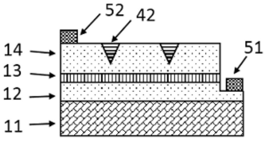
[0031] refer to figure 1 , in the horizontal device structure, the positive electrode 52 is located on the top of the p-GaN14, and the three-dimensional cavity 41 is opened on the upper surface of the p-GaN14, and the negative electrode 51 is located above the n-GaN12. During the preparation, the three-dimensional cavity 41 is prepared first , and then prepare the positive electrode 52 and the negative electrode 51, wherein, the n-GaN12 is exposed by ICP etching for the preparation of the negative electrode 51.

Embodiment 2

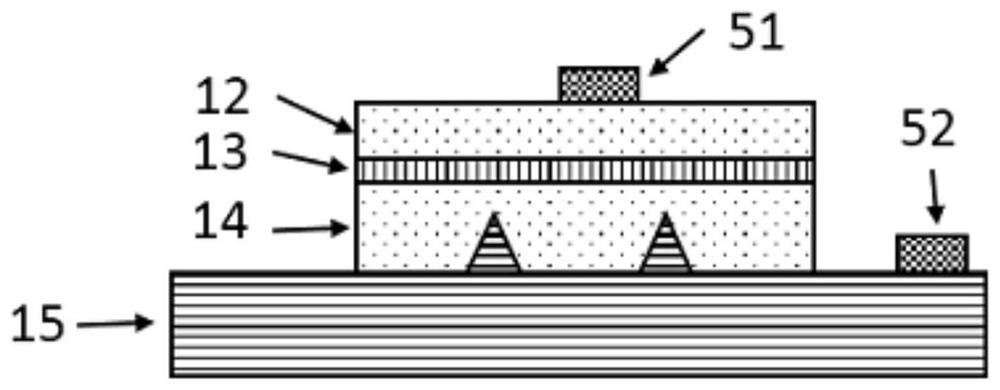
[0033] refer to figure 2 , in the vertical structure device, the positive electrode 52 is located on the transfer substrate 15, and the three-dimensional cavity 41 is opened on the surface of p-GaN14. During the preparation, the three-dimensional cavity 41 is prepared first, and then the transfer substrate is realized by bonding and laser lift-off. 15, the three-dimensional cavity 41 is located on the back of the light-emitting surface.

Embodiment 3

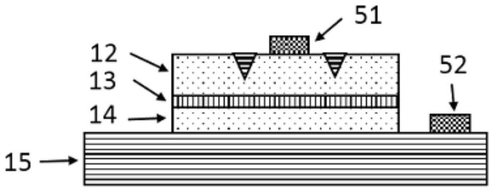
[0035] refer to image 3 , in the vertical structure device, the positive electrode 52 is located on the transfer substrate 15, and the three-dimensional cavity 41 is opened on the surface of n-GaN12. During the preparation, the transfer of the transfer substrate 15 is first realized by bonding and laser lift-off, and then the three-dimensional cavity 41 is carried out. The three-dimensional cavity 41 is located in front of the light-emitting surface.

[0036] The invention can be used for gallium nitride-based light-emitting devices of various types and in various bands, and can also be used for optoelectronic devices of semiconductor materials; Both excitation modes of electric pumping are applicable.


PUM

PropertyMeasurementUnit
sizeaaaaaaaaaa

Abstract

The invention discloses a GaN-based semiconductor light-emitting device enhanced by a three-dimensional cavity hyperbolic metamaterial, comprising a substrate, a GaN epitaxial layer, a negative electrode and a positive electrode, wherein the GaN epitaxial layer covers the substrate, and the surface of the GaN epitaxial layer A three-dimensional cavity is opened on it, and the three-dimensional cavity is filled with a hyperbolic metamaterial to form a three-dimensional cavity hyperbolic structure. The negative electrode is located on the surface of n-GaN, and the positive electrode is located on the transfer substrate or the surface of p-GaN. Semiconductor light-emitting devices can realize the improvement of quantum efficiency and light extraction efficiency in a specific spectral range.

Description

technical field [0001] The invention belongs to the technical field of semiconductors, and relates to a GaN-based semiconductor light-emitting device enhanced by a three-dimensional cavity hyperbolic metamaterial. Background technique [0002] The luminescence range of group III nitride semiconductor materials can extend from the near-infrared region to the ultraviolet region, which makes it of great application value in various types of light-emitting devices such as lighting, display, and optical communication. However, the excellent properties of nitride semiconductor materials have not been fully utilized, especially in high-brightness and high-speed modulation white LEDs, high-resolution displays, and high-performance deep ultraviolet light-emitting devices, there is still a lot of room for development. This is mainly due to the low quantum efficiency of the device caused by the difficulty in the preparation of high-aluminum and high-indium component materials and the l...

Claims


Application Information

Patent Timeline
Patent Type & Authority Patents(China)
IPC IPC(8): H01L33/20H01L33/14
CPCH01L33/14H01L33/20
Inventor 田振寰云峰张明殷王旭正
Owner XI AN JIAOTONG UNIV
Why Eureka
Try Eureka