Chip detection device based on image recognition

A technology of chip detection and image recognition, applied in measurement devices, material analysis through optical means, instruments, etc., can solve the problems of eye fatigue, error-prone, heavy work intensity and damage of microscope inspection personnel

Inactive Publication Date: 2019-09-13
丽水奇异果信息技术有限公司
View PDF6 Cites 13 Cited by
  • Summary
  • Abstract
  • Description
  • Claims
  • Application Information

AI Technical Summary

Problems solved by technology

The maturity of the IC will bring about a great leap forward in technology, whether it is in design technology or semiconductor process breakthroughs, both are closely related, so the requirements for chip processing and manufacturing are increasing day by day, but the process production steps of chips are especially important. One of the important process steps is microscopic inspection to eliminate

Method used


Image

  • Chip detection device based on image recognition
  • Chip detection device based on image recognition
  • Chip detection device based on image recognition

Examples


Embodiment Construction

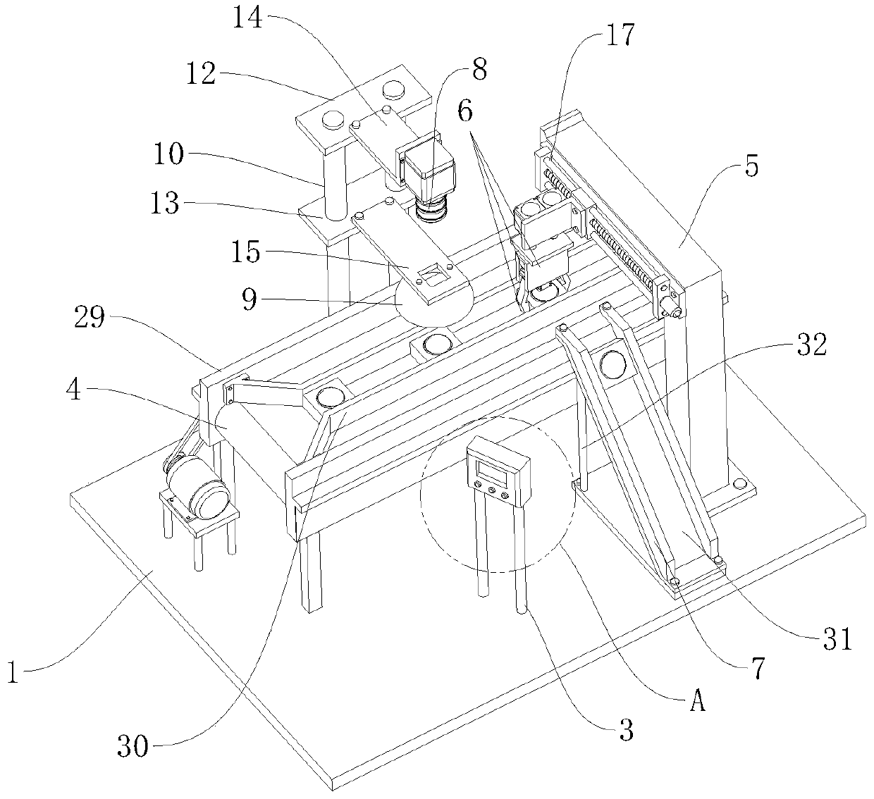
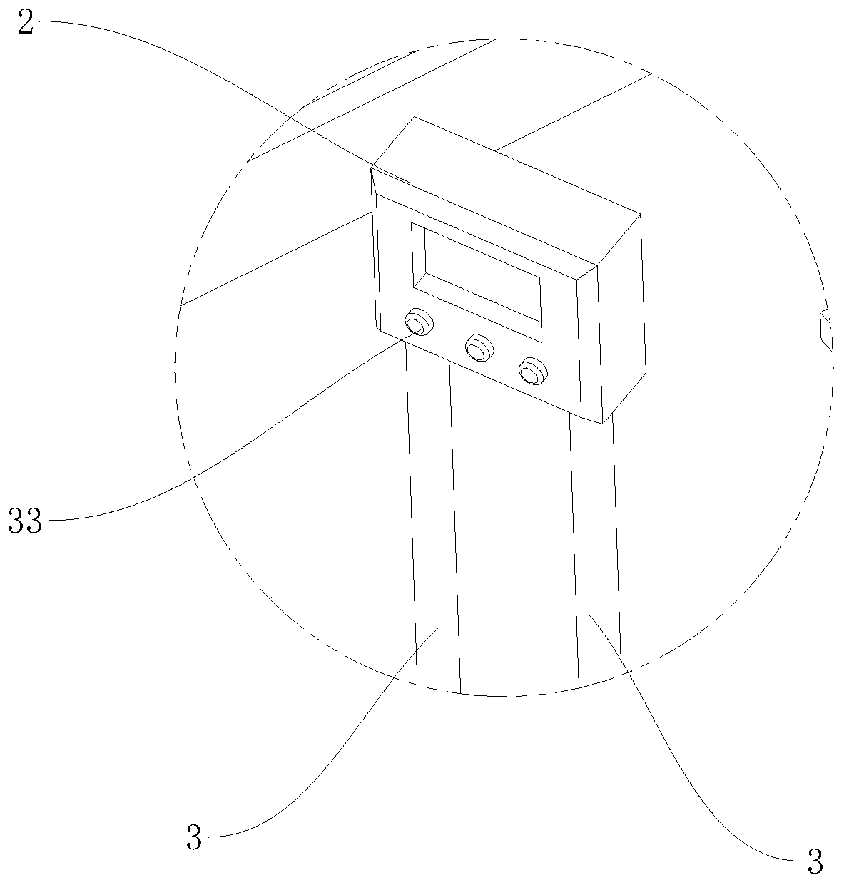
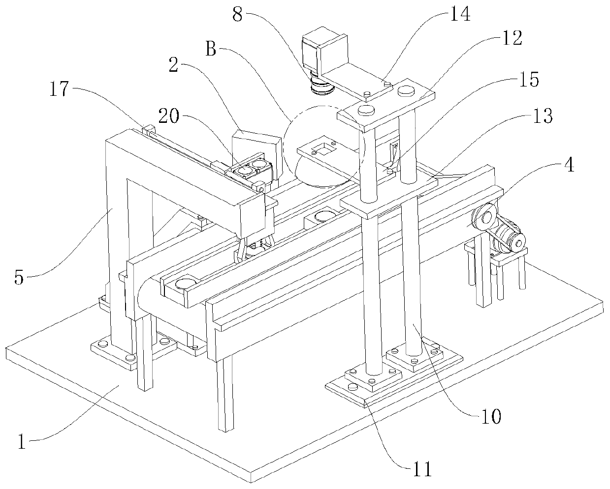
[0023] The technical solutions of the present invention will be further described below in conjunction with the accompanying drawings and through specific implementation methods.

[0024] Wherein, the accompanying drawings are only for illustrative purposes, showing only schematic diagrams, rather than physical drawings, and should not be construed as limitations on this patent; in order to better illustrate the embodiments of the present invention, some parts of the accompanying drawings will be omitted, Enlargement or reduction does not represent the size of the actual product; for those skilled in the art, it is understandable that certain known structures and their descriptions in the drawings may be omitted.

[0025] In the drawings of the embodiments of the present invention, the same or similar symbols correspond to the same or similar components; , "inner", "outer" and other indicated orientations or positional relationships are based on the orientations or positional ...


PUM


Abstract

The invention relates to the field of detection devices, in particular to a chip detection device based on image recognition. The chip detection device comprises a base and a control desk and furthercomprises a conveyor, a detection mechanism and a discharge mechanism. The discharge mechanism comprises a reversed-L-shaped supporting plate, a clamping assembly and a slide way. The reversed-L-shaped supporting plate is vertically arranged on the top of the base. The bottom of the reversed-L-shaped supporting plate is fixedly connected with the top of the base. The clamping assembly is movably arranged on one side wall of the reversed-L-shaped supporting plate. The slide way is arranged beside the reversed-L-shaped supporting plate in an inclined manner. The chip detection device based on image recognition is used before the microscopic examination work, the number of defective products in the chip mass production can be decreased through the image recognition principle, the mistake occurrence probability in chip detection is also decreased while the work intensity of microscopic examination workers is lowered, and therefore the work efficiency is improved, the chip quality is further improved, and benefits are increased.

Description

technical field [0001] The invention relates to the field of detection equipment, in particular to a chip detection device based on image recognition. Background technique [0002] Chip is the general term for semiconductor component products, also known as integrated circuits, or microcircuits, microchips, chips / chips. In electronics, it is a way to miniaturize circuits (mainly including semiconductor equipment, including passive components, etc.). and is often fabricated on the surface of a semiconductor wafer. Only half a century after its development, integrated circuits became ubiquitous, with computers, cell phones and other digital appliances becoming an integral part of the fabric of society. That's because modern computing, communication, manufacturing and transportation systems, including the Internet, all rely on the existence of integrated circuits. Even many scholars believe that the digital revolution brought about by integrated circuits is the most important...

Claims


Application Information

Patent Timeline
IPC IPC(8): B07C5/00B07C5/02B07C5/36G01N21/956
CPCB07C5/00B07C5/02B07C5/362G01N21/956G01N21/95607G01N2021/95615G01N2021/95638
Inventor 朱海艳
Owner 丽水奇异果信息技术有限公司
Why Eureka
Try Eureka