Semiconductor device

A semiconductor, conductive type technology, applied in the direction of semiconductor devices, transistors, electric solid devices, etc., can solve the problems of easy breakdown, heightening and damage of the peripheral part

Active Publication Date: 2019-09-17
DENSO CORP
View PDF6 Cites 0 Cited by
  • Summary
  • Abstract
  • Description
  • Claims
  • Application Information

AI Technical Summary

Problems solved by technology

Therefore, in the above-mentioned semiconductor device, when the current is interrupted from the state where the current is flowing, breakdown is likely to occur in the outer peripheral portion.
In addition, since the above-mentioned semiconductor device is less likely to allow current to flow out in the outer peripheral portion than in the element portion, if a breakdown occurs in the outer peripheral portion, the possibility of damage becomes high.

Method used


Image

  • Semiconductor device
  • Semiconductor device
  • Semiconductor device

Examples


no. 1 Embodiment approach

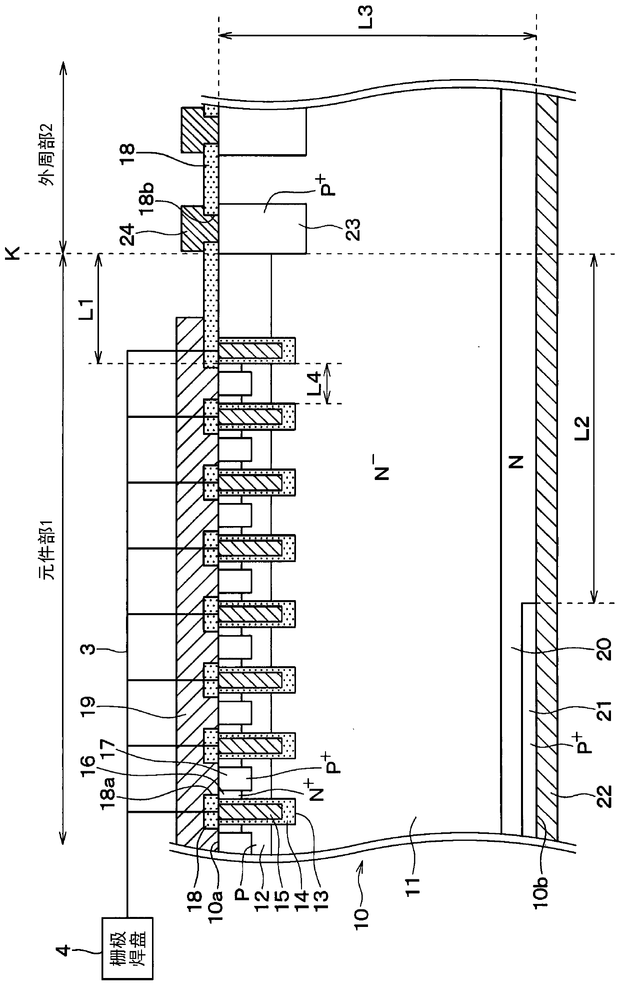
[0026] refer to figure 1 The semiconductor device of the first embodiment will be described. Such as figure 1 As shown, the semiconductor device of this embodiment includes a semiconductor substrate 10 having one surface 10a and the other surface 10b opposite to the one surface 10a, and an element portion 1 in which an IGBT element is formed and an outer peripheral portion 2 surrounding the element portion 1 are formed. . First, the basic structure of the element unit 1 will be described.

[0027] Component part 1 has N - A P-type drift layer 11, and a P-type base layer 12 is formed on the drift layer 11 (that is, on the side 10a of the semiconductor substrate 10). In addition, a plurality of trenches 13 penetrating the base layer 12 and reaching the drift layer 11 are formed, and the base layer 12 is divided by the plurality of trenches 13 . In this embodiment, the plurality of trenches 13 is along one of the plane directions of the one side 10a of the semiconductor subs...

no. 2 Embodiment approach

[0064] A second embodiment will be described. With respect to the first embodiment, in this embodiment, a part of the plurality of gate electrodes 15 is connected to the gate pad 4, and the remaining part of the plurality of gate electrodes 15 is connected to the upper electrode 19, and the others are the same as those of the first embodiment. It is the same, so the description is omitted here.

[0065] In this embodiment, if Image 6 As shown, some gate electrodes 15 a among the plurality of gate electrodes 15 are connected to the gate pad 4 . Furthermore, the remaining gate electrodes 15 b among the plurality of gate electrodes 15 are not connected to the gate pad 4 , but are connected to the upper electrode 19 through the third contact hole 18 c formed in the interlayer insulating film 18 . That is, the gate electrode 15 b connected to the upper electrode 19 is a so-called dummy gate electrode that does not function as an inversion layer in the base layer 12 when the semi...


PUM


Abstract

This semiconductor device has an element part (1) and an outer peripheral part (2) surrounding the element part (1), wherein a deep layer (23) is formed more deeply in the outer peripheral part (2) than in a base layer (12). When the position which, in the deep layers (23), is closest to the element part (1) is a boundary position (K), the distance between the boundary position (K) and the position which is closest to the outer peripheral part (2) in an emitter region (16) into which first carriers can be injected is a first distance (L1), and the distance between the boundary position (K) and the position of a stepped part in a surface direction of a semiconductor substrate (10) in a collector layer (21) is a second distance (L2), the first distance (L1) and the second distance (L2) are adjusted so that a carrier density at the outer peripheral part (2) is decreased on the basis of the withstand voltage of the outer peripheral part (2), the withstand voltage having been decreased by the deep layer (23).

Description

[0001] Cross-reference of connected application [0002] This application is based on Japanese Patent Application No. 2017-18672 filed on February 3, 2017, and the description thereof is incorporated herein by reference. technical field [0003] The present invention relates to a semiconductor device having an element portion in which an insulated gate bipolar transistor (hereinafter referred to as “IGBT”) element is formed, and an outer peripheral portion surrounding the element portion. Background technique [0004] Conventionally, a semiconductor device having an element portion in which an IGBT element is formed and a peripheral portion surrounding the element portion has been proposed (for example, refer to Patent Document 1). Specifically, this semiconductor device includes a semiconductor substrate having one surface and another surface opposite to the one surface and constituting a drift layer. In addition, in the element portion, a P-type base layer is formed on th...

Claims


Application Information

Patent Timeline
Patent Type & Authority Applications(China)
IPC IPC(8): H01L29/78H01L29/06H01L29/739
CPCH01L29/4236H01L29/36H01L29/7397H01L29/1095H01L29/404H01L29/0619H01L29/4238H01L29/42376H01L29/0834H01L29/0623H01L29/06H01L29/7371H01L29/6634H01L29/7395H01L29/0607H01L27/0823H01L29/732H01L29/66333H01L29/0821
Inventor 宫田征典高桥茂树住友正清志贺智英
Owner DENSO CORP
Why Eureka
Try Eureka