Supercharge Your Innovation With Domain-Expert AI Agents!

Memory cell array peripheral circuit and memory device

A storage cell array and peripheral circuit technology, applied in the field of memory, can solve problems such as excessive peripheral circuit area, and achieve the effect of reducing the occupied area and the area

Active Publication Date: 2019-09-24
YANGTZE MEMORY TECH CO LTD
View PDF7 Cites 2 Cited by
  • Summary
  • Abstract
  • Description
  • Claims
  • Application Information

AI Technical Summary

Problems solved by technology

[0005] In view of this, the embodiment of the present application provides a memory cell array peripheral circuit and a memory device, which can solve the problem of excessive peripheral circuit area in the prior art

Method used


Image

  • Memory cell array peripheral circuit and memory device
  • Memory cell array peripheral circuit and memory device
  • Memory cell array peripheral circuit and memory device

Examples


Embodiment Construction

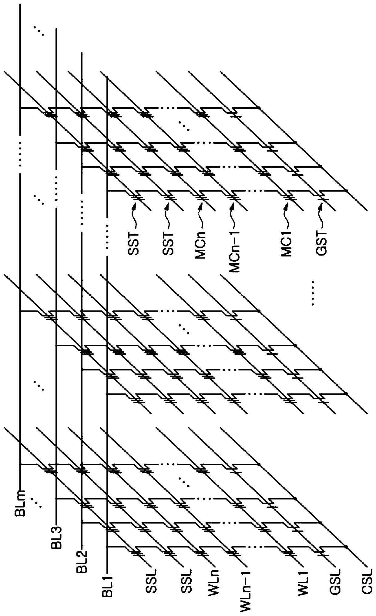
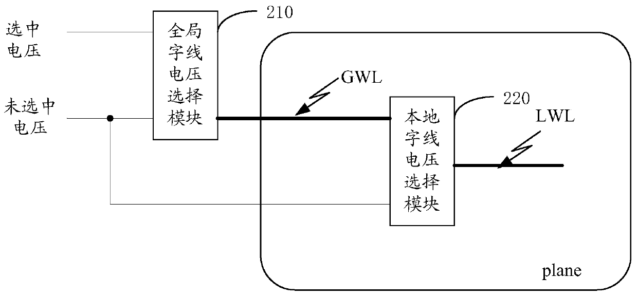
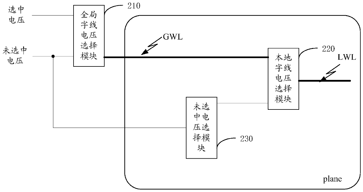
[0033] In order to enable those skilled in the art to better understand the solutions of this application, the technical solutions in the embodiments of this application will be clearly and completely described below in conjunction with the drawings in the embodiments of this application. Obviously, the described embodiments are only It is a part of the embodiments of this application, not all of the embodiments. Based on the embodiments in this application, all other embodiments obtained by those of ordinary skill in the art without creative work shall fall within the protection scope of this application.

[0034] It should be understood that in this application, "at least one (item)" refers to one or more, and "multiple" refers to two or more. "And / or" is used to describe the association relationship of associated objects, indicating that there can be three types of relationships, for example, "A and / or B" can mean: only A, only B, and both A and B , Where A and B can be singu...


PUM


Abstract

The embodiment of the invention discloses a memory cell array peripheral circuit and a memory device, the memory cell array comprises a plurality of memory cell planes, and each memory cell plane comprises M local word lines; each global word line in the peripheral circuit corresponds to a plurality of local word lines on each storage unit plane and is in one-to-one correspondence with the global word line voltage selection modules; the local word line voltage selection modules are in one-to-one correspondence with the local word lines; the global word line voltage selection module selects one voltage from the selected voltage and the unselected voltage and outputs the voltage to the input end of the corresponding local word line voltage selection module through the corresponding global word line; and the local word line voltage selection module selects one voltage from the voltage output by the corresponding global word line voltage selection module and the unselected voltage and outputs the selected voltage to the corresponding local word line. Due to the fact that the local word lines share one global word line, the occupied area of the required multiplexer is reduced, and the area of a peripheral circuit can be reduced.

Description

Technical field [0001] This application relates to the field of memory technology, and in particular to a peripheral circuit of a memory cell array and a storage device. Background technique [0002] NAND Flash storage devices are non-volatile storage products with low power consumption, light weight and good performance, and are widely used in electronic products. With the advent of the era of big data, the planar structure of NAND devices has approached the limit of actual expansion. In order to further increase the storage capacity and reduce the storage cost per bit, 3D NAND Flash memory is proposed. [0003] In 3D NAND Flash memory, such as figure 1 As shown, a plurality of memory cell tubes (memory cells) are connected in series via bit lines (BL) to form a memory cell string. The memory cell strings str are arranged in a three-dimensional direction to form a memory cell array. One end is also connected to a page buffer via BL, and different memory cell tubes along the memor...

Claims


Application Information

Patent Timeline
IPC IPC(8): G11C16/08G11C16/04
CPCG11C16/0483G11C16/08
Inventor 王瑜阮庆
Owner YANGTZE MEMORY TECH CO LTD
Features
  • R&D
  • Intellectual Property
  • Life Sciences
  • Materials
  • Tech Scout
  • Unparalleled Data Quality
  • Higher Quality Content
  • 60% Fewer Hallucinations
Learn More