

Wireless charging device and protection circuit thereof
A technology for wireless charging equipment and protection circuits, applied in the electronic field, can solve problems such as damage to battery packs, voltage rise in the rear stage, etc., achieve safe and reliable circuits, and solve the effects of battery packs and charging equipment
- Summary
- Abstract
- Description
- Claims
- Application Information
AI Technical Summary
Problems solved by technology
Method used
Image

Examples
Embodiment 1
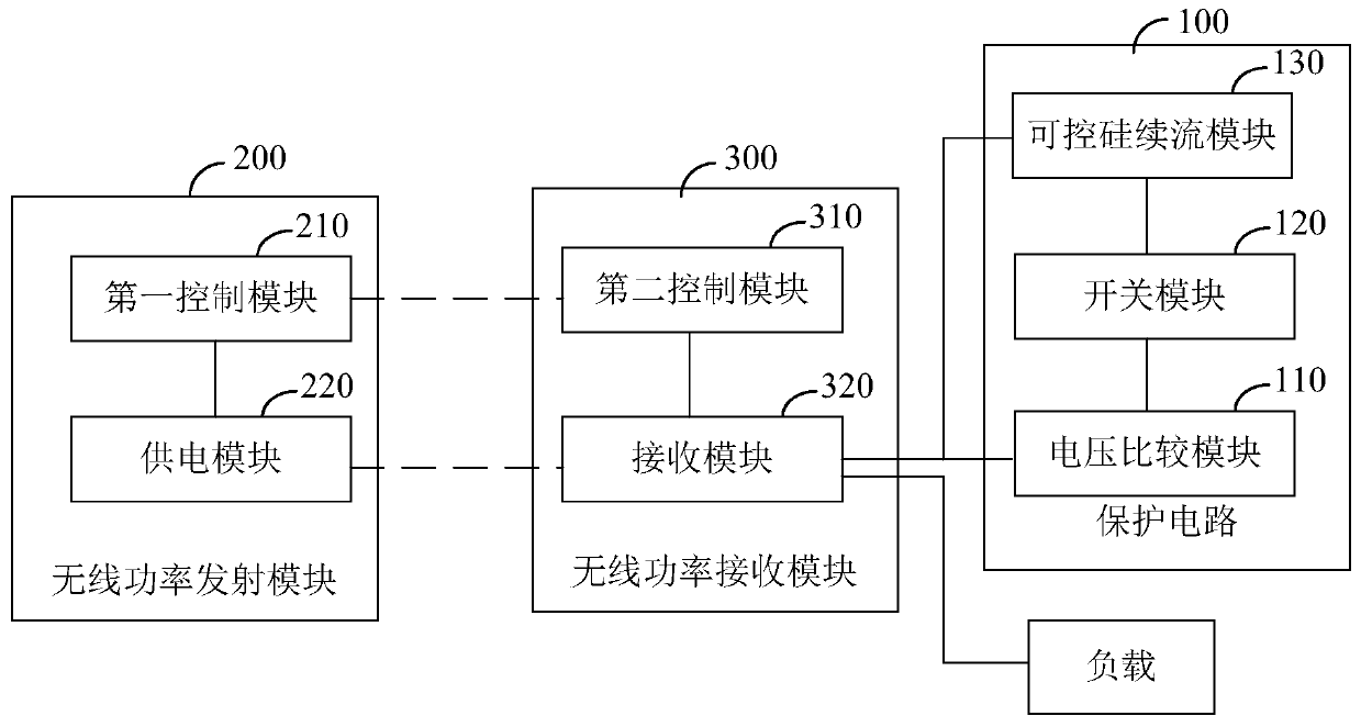
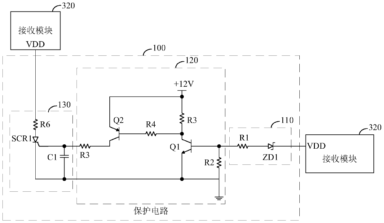
[0021] figure 1 The structure of the protection circuit of the wireless charging device provided by Embodiment 1 of the present invention is shown. For the convenience of description, only the parts related to the embodiment of the present invention are shown. The details are as follows:
[0022] see figure 1 , a protection circuit 100 for a wireless charging device provided in an embodiment of the present invention is used for connecting with a wireless power receiving module of the wireless charging device. The above wireless charging device includes a wireless power sending module 200 and a wireless power receiving module 300, the wireless power sending module 200 includes a first control module 210 and a power supply module 220, the wireless power receiving module 300 includes a second control module 310 and a receiving module 320, receiving The output end of the module 320 is connected to the load (battery pack), and the first control module 210 is connected to the secon...
Embodiment 2
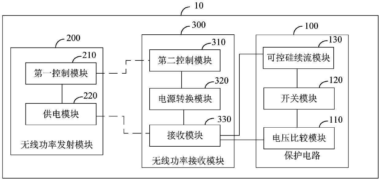
[0046] The wireless charging device 10 provided by Embodiment 2 of the present invention. The above wireless charging device 10 includes a wireless power transmitting module 200 , a wireless power receiving module 300 wirelessly connected to the wireless power transmitting module 200 , and the protection circuit 100 described in the first embodiment.
[0047] The wireless power transmission module 200 includes a first control module 210 and a power supply module 220, the power receiving module 300 includes a second control module 310, a power conversion module 320 and a receiving module 330, the voltage output terminal of the receiving module 330 is connected to a load, The first control module 210 is connected to the second control module 310 in communication, and the protection circuit 100 is connected to the power conversion module 320 .
PUM
 Abstract
Description
Claims
Application Information