Substrate suction device and semiconductor processing equipment

A technology for sucking device and substrate, applied in semiconductor/solid-state device manufacturing, electrical components, circuits, etc., can solve problems such as substrate crushing and large substrate deformation, and achieve the effect of avoiding damage

Inactive Publication Date: 2019-10-11
BEIJING NAURA MICROELECTRONICS EQUIP CO LTD
View PDF8 Cites 2 Cited by
  • Summary
  • Abstract
  • Description
  • Claims
  • Application Information

AI Technical Summary

Problems solved by technology

[0004] The above-mentioned existing substrate suction device has the following problems in practical application: since the pumping chamber corresponds to the central area of ​​the substrate, the large vacuum adsorption force here will cause large deformation of the substrate, thereby easily causing substrate crush

Method used


Image

  • Substrate suction device and semiconductor processing equipment
  • Substrate suction device and semiconductor processing equipment
  • Substrate suction device and semiconductor processing equipment

Examples


Embodiment 1

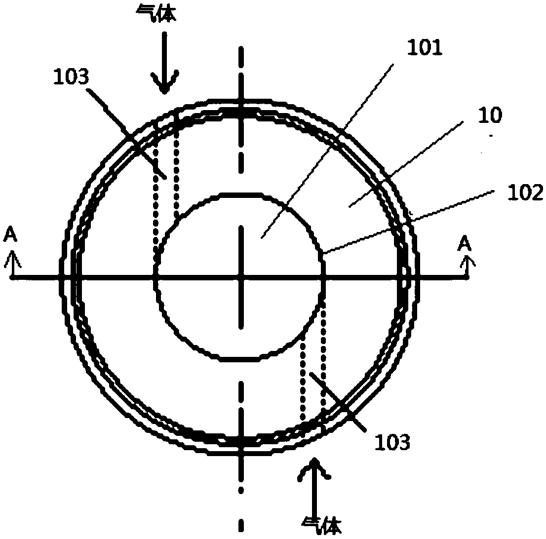
[0029] Figure 3a A top view of the substrate suction device provided in Embodiment 1 of the present invention; Figure 3b A cross-sectional view of the substrate pick-up device provided in Embodiment 1 of the present invention; Figure 4 for Figure 3a and Figure 3b Schematic diagram of the substrate pick-up setup shown; see also Figure 3a , 3b And 4, the substrate suction device provided by the embodiment of the present invention includes: a body 10; a cavity 101 with an opening 102 at the lower end is formed in the body 10; an air inlet 103 communicating with the cavity 101 is provided at the upper end of the body 10 , the inlet hole 103 is used to be connected with the compressed gas source, so that the compressed gas provided by the compressed gas source enters the cavity 101 from the inlet hole 103 to form a vortex air flow and is discharged from the opening 102 (the gas is in a spiral shape under the action of air pressure. shape gradually moves downward, and fin...

Embodiment 2

[0033] Compared with the substrate suction device provided in the embodiment 1 of the present invention, the substrate suction device provided in the embodiment of the present invention can be found in Figure 5-7 , also including the main body 10, since the main body 10 has been described in detail in the above-mentioned embodiment 1, it will not be repeated here.

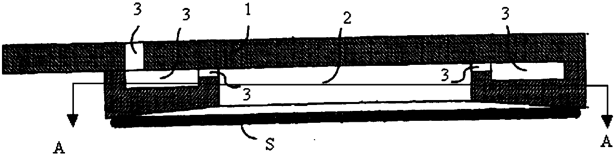
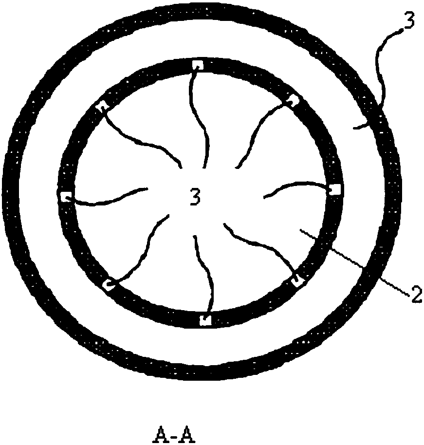
[0034] Only the differences between this embodiment and the above-mentioned Embodiment 1 will be described below. Specifically, the number of bodies 10 in the substrate pick-up device provided in Embodiment 2 is multiple; the multiple bodies 10 correspond to different regions of the substrate S, so as to absorb and fix different regions of the substrate S correspondingly. In this way, The problem of unstable adsorption caused by the limited adsorption force of the single body 10 can be avoided. The unstable adsorption includes: the orientation of the substrate S cannot be controlled when the substrate S rotates wi...

Embodiment 3

[0047] An embodiment of the present invention provides a semiconductor processing device, including: a substrate pick-up device and a transfer device; the substrate pick-up device adopts the substrate pick-up device provided in Embodiments 1 and 2 above to fix the substrate; the transfer device is used to control The substrate pick-up moves to indirectly transport the substrates.

[0048] The semiconductor processing equipment provided by the embodiment of the present invention adopts the substrate suction device provided by the above-mentioned embodiments 1 and 2, so problems such as damage and deformation to the surface of the substrate during substrate transfer can be avoided.


PUM


Abstract

The invention provides a substrate suction device. The substrate suction device comprises a body. A cavity with an opening at the lower end is formed in the body; an air inlet hole communicated with the cavity is formed in the upper end of the body; the air inlet hole is connected with a compressed air source, and the compressed air provided by the compressed air source enters the cavity from theair inlet hole to form vortex air flow and is discharged from the opening; and the vortex air flow enables the central area of the cavity to be a negative pressure area, so that the substrate locatedbelow the opening and having a preset gap with the opening is adsorbed and fixed. The invention also provides semiconductor processing equipment. The substrate suction device is a non-contact substrate fixing device, and can avoid the problems of damage, deformation and the like on the surface of a substrate when the substrate is conveyed.

Description

technical field [0001] The invention belongs to the technical field of semiconductor processing equipment, and in particular relates to a substrate suction device and semiconductor processing equipment. Background technique [0002] The front side of the substrate refers to the substrate surface used to form the integrated circuit structure, and the ring-shaped area of ​​the front side a few millimeters from the edge is usually not used to realize integrated circuit manufacturing. Therefore, the front side of the substrate needs to be protected during the substrate transfer process. It is not damaged, so it is generally selected to carry out the substrate through the back of the supporting substrate, but this situation is only applicable to some processes, for example, the etching of the IC process line and the PVD deposition process are not applicable to certain process conditions Under, for example, silicon epitaxial CVD processes, in which case the edge transfer substrate...

Claims


Application Information

Patent Timeline
Patent Type & Authority Applications(China)
IPC IPC(8): H01L21/683H01L21/67
CPCH01L21/6838H01L21/67011
Inventor 刘凯
Owner BEIJING NAURA MICROELECTRONICS EQUIP CO LTD
Why Eureka
Try Eureka