LED panel and display device

A display device, LED chip technology, applied in the direction of electrical components, electrical solid devices, circuits, etc., can solve the problems of low production efficiency, achieve the effects of improving production efficiency, reducing welding failures, and reducing welding failures

Active Publication Date: 2019-10-11
HISENSE VISUAL TECH CO LTD
View PDF9 Cites 2 Cited by
  • Summary
  • Abstract
  • Description
  • Claims
  • Application Information

AI Technical Summary

Problems solved by technology

[0007] The present invention provides an LED board and a display device to solve the problem of low production efficiency in the production process of Mini LED boards existing in the prior art

Method used


Image

  • LED panel and display device
  • LED panel and display device
  • LED panel and display device

Examples


Embodiment Construction

[0061] In order to make the object, technical solution and advantages of the present invention clearer, the present invention will be further described in detail below in conjunction with the accompanying drawings. Obviously, the described embodiments are only some embodiments of the present invention, rather than all embodiments . Based on the embodiments of the present invention, all other embodiments obtained by persons of ordinary skill in the art without making creative efforts belong to the protection scope of the present invention.

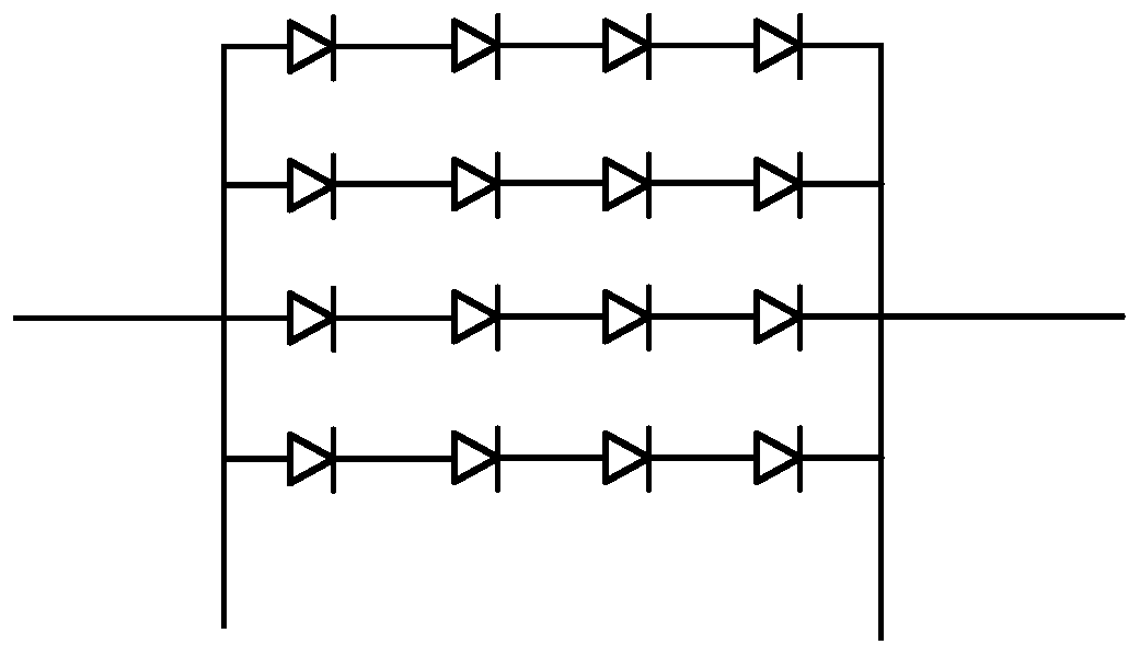
[0062] The Mini LED backlight panel adopts partition settings, the Mini LEDs in the zone are connected in series, and the zones are connected in parallel. If one Mini LED is not welded properly, all the Mini LEDs in the zone will not light up.

[0063] Such as figure 1 Shown is a schematic structural diagram of the Mini LED backlight display circuit schematic. figure 1 , only a part of the schematic diagram of the MiniLED backlight circui...


PUM


Abstract

The invention discloses an LED panel and a display device, which are used for solving the problem that in the prior art, the production efficiency is low in the production process of MiniLED panels. The LED panel comprises a substrate and an LED chip formed on the substrate; a bonding pad assembly corresponding to the LED chip is arranged on the substrate; and in a pair of the LED chip and the bonding pad assembly which correspond to each other, bonding pad gaps with at least two sizes are formed between a positive electrode bonding pad set and a negative electrode bonding pad set of the bonding pad assembly, and the LED chip is welded on the bonding pad assembly through the bonding pad gap with one size. Due to the fact that the bonding pad gaps with the at least two sizes exist, the bonding pad gap of one size can be selected from the bonding pad gaps with the at least two sizes, and the LED chip is welded on the bonding pad assembly through the selected bonding pad gap with one size, so that poor welding is reduced and the production efficiency is improved; and the maintenance is carried out directly through other bonding pad gaps during maintenance, so that the maintenance difficulty is reduced.

Description

technical field [0001] The invention relates to the field of display technology, in particular to an LED panel and a display device. Background technique [0002] Mini LED (Mini Light Emitting Diode, miniature light-emitting diode) has become a current hot spot in LCD (Liquid Crystal Display, liquid crystal display) display as a backlight. A huge number of Mini LED grains are used as the backlight source. This solution has the advantages of adjustable regional brightness, high color rendering and contrast, and can achieve 8K display effect. Multi-zone dynamic backlighting due to high peak brightness LEDs contributes to improved display contrast and high dynamic range. Therefore, Mini LED as a technical solution for backlighting has been applied in many fields such as TV, mobile phone, and vehicle display. [0003] Mini LED chips need to be soldered to a substrate to form a Mini LED board. During the soldering process, if the pad spacing of the Mini LED chip is equal to th...

Claims


Application Information

Patent Timeline
Patent Type & Authority Applications(China)
IPC IPC(8): H01L33/62H01L25/075
CPCH01L25/0753H01L33/62H01L2933/0066
Inventor 李富琳唐兆兵乔明胜
Owner HISENSE VISUAL TECH CO LTD
Why Eureka
Try Eureka