Laser irradiation device, thin-film transistor manufacturing method, program, and projection mask
A thin-film transistor and laser irradiation technology, which is applied in the direction of transistors, semiconductor/solid-state device manufacturing, lasers, etc., can solve the problems of small electron mobility and charge mobility, and achieve the effect of suppressing fluctuations and reducing characteristic deviations
- Summary
- Abstract
- Description
- Claims
- Application Information
AI Technical Summary
Problems solved by technology
Method used
Image

Examples
no. 1 approach
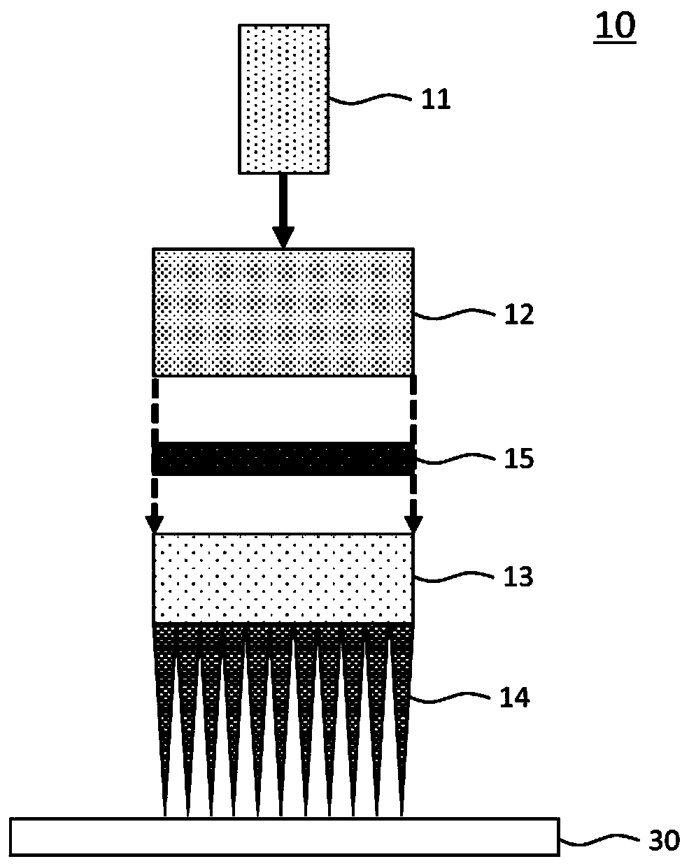
[0047] figure 1 It is a figure which shows the structural example of the laser irradiation apparatus 10 in 1st Embodiment of this invention.
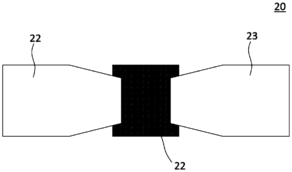
[0048] In the first embodiment of the present invention, the laser irradiation device 10 is used in the manufacturing process of a semiconductor device such as a thin film transistor (TFT) 20 , for example, to irradiate a region where a channel region is to be formed and perform annealing, so that the channel region The channel region forms a device in which a predetermined region is polycrystallized.
[0049] The laser irradiation device 10 is used, for example, when forming a thin film transistor of a pixel such as a peripheral circuit of a liquid crystal display device. When forming such a thin film transistor, first, a gate electrode made of a metal film such as Al is patterned on the substrate 30 by sputtering. Then, a gate insulating film made of a SiN film is formed on the entire surface of the substrate 30 by a low-temperature...
no. 2 approach
[0082] In the second embodiment of the present invention, a part of the laser light passing through the peripheral region (edge region) of the projection mask is blocked by providing a plurality of light shielding portions. Accordingly, the energy of the laser light in the peripheral region of the projection mask 150 is reduced, and the energy of the laser light in the entire channel region can be made uniform.
[0083] Since the configuration example of the laser irradiation device of the second embodiment and figure 1 The laser irradiation device 10 of the illustrated first embodiment is the same, and therefore detailed description thereof will be omitted.
[0084] If the laser is irradiated without setting the shading part, then if Figure 6 As shown, in the channel region, the energy of the laser beam passing through the edge region of the transmission region 151 becomes larger, which causes the crystallization speed of the edge region to increase. Therefore, in the se...
no. 3 approach
[0092] In the third embodiment of the present invention, the energy of the laser light in the channel region is made uniform by providing an auxiliary pattern on the projection mask and also providing a light-shielding part inside the transmissive part.
[0093] Since the configuration example of the laser irradiation device according to the third embodiment and figure 1 The laser irradiation device 10 of the illustrated first embodiment is the same, and therefore detailed description thereof will be omitted.
[0094] Figure 11 It is a figure which shows the structural example of the projection mask 150 of 3rd Embodiment.
[0095] Such as Figure 11 As shown in (a), the projection mask 150 is provided with the auxiliary pattern 153 along the longitudinal direction of the transmissive region 151 , and the light shielding portion 154 is provided in the edge region (region α) of the transmissive region 151 in the width direction.
[0096] Regarding the long side direction of ...
PUM
 Abstract
Description
Claims
Application Information
 - R&D Engineer
- R&D Manager
- IP Professional
- Industry Leading Data Capabilities
- Powerful AI technology
- Patent DNA Extraction
Browse by: Latest US Patents, China's latest patents, Technical Efficacy Thesaurus, Application Domain, Technology Topic.
© 2024 PatSnap. All rights reserved.Legal|Privacy policy|Modern Slavery Act Transparency Statement|Sitemap