
Laminated structure used for three-dimensional memory, three-dimensional memory and preparation method thereof

A stacked structure and memory technology, which is applied in semiconductor/solid-state device manufacturing, electric solid-state devices, semiconductor devices, etc., can solve problems such as poor coupling effect of erased state, fast programming/erasing speed, inconsistent characteristics of memory storage units, etc.

Inactive Publication Date: 2019-10-18
YANGTZE MEMORY TECH CO LTD
View PDF4 Cites 1 Cited by
  • Summary
  • Abstract
  • Description
  • Claims
  • Application Information

AI Technical Summary

Problems solved by technology

[0003] In view of the above-mentioned shortcomings of the prior art, the purpose of the present invention is to provide a stacked structure for a three-dimensional memory, a three-dimensional memory and a preparation method thereof, which are used to solve the existing problem of the three-dimensional memory in the prior art corresponding to channel communication. Compared with the memory cells corresponding to the larger portion of the channel via width, the memory cells with a smaller hole width are programmed / erased faster, and the memory cells corresponding to the smaller portion of the channel via hole width are more severely read. The coupling effect of the erased state is poor, and the characteristics of the memory cells in each part of the memory are inconsistent, resulting in a wide distribution of the threshold voltage of the three-dimensional memory, thereby affecting the performance of the three-dimensional memory, etc.

Method used


Image

  • Laminated structure used for three-dimensional memory, three-dimensional memory and preparation method thereof
  • Laminated structure used for three-dimensional memory, three-dimensional memory and preparation method thereof
  • Laminated structure used for three-dimensional memory, three-dimensional memory and preparation method thereof

Examples


Embodiment 1

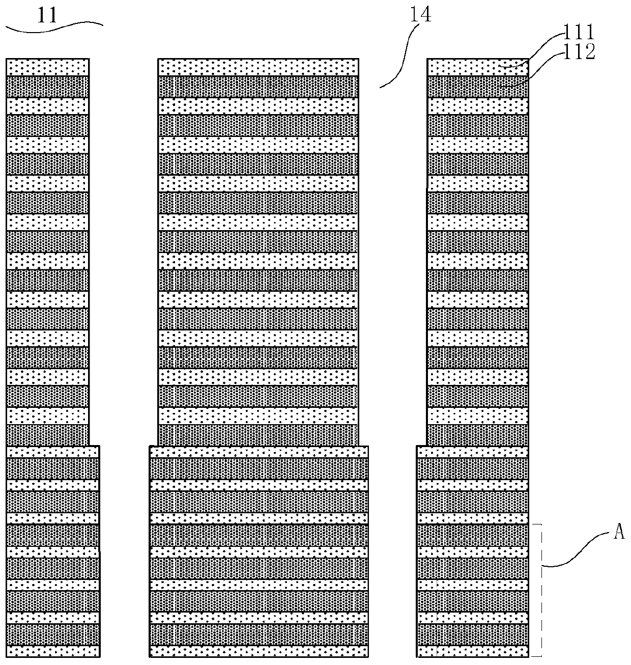
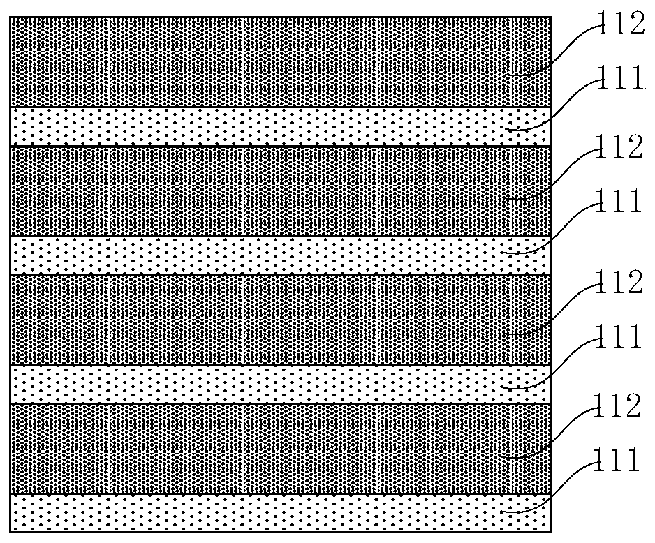
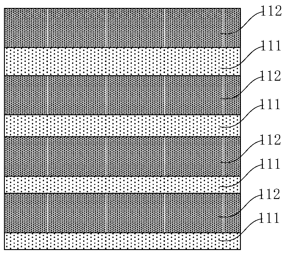
[0120] see figure 1 , the present invention provides a stacked structure 11 for a three-dimensional memory, the stacked structure 11 for a three-dimensional memory includes sacrificial layers 111 and inter-gate dielectric layers 112 alternately stacked up and down; A channel via hole 14 penetrating through the laminated structure 11 along the thickness direction of the laminated structure 11 is formed. Along the thickness direction of the laminated structure 11, the width of each part of the channel via hole 14 varies. The same; the thickness of the sacrificial layer is proportional to the width of the trench hole 14 .

[0121] As an example, the laminated structure 11 can be divided into an upper part and a lower part from top to bottom along the thickness direction of the laminated structure 11, and the ratio of the upper part of the laminated structure 11 to the total thickness of the laminated structure 11 is It can be set according to actual needs; similarly, the ratio o...

Embodiment 2

[0133] see Figure 11 The present invention also provides a stacked structure 12 for a three-dimensional memory, the stacked structure 12 includes gate layers 121 and inter-gate dielectric layers 112 alternately stacked up and down; The thickness direction of the stacked structure 12 runs through the channel via hole 14 of the stacked structure 12, and along the thickness direction of the stacked structure 12, the width of each part of the channel via hole 14 is different; The thickness of the gate layer 121 is proportional to the width of the channel via hole 14 .

[0134] As an example, the laminated structure 12 can be divided into an upper part and a lower part from top to bottom along the thickness direction of the laminated structure 11, and the ratio of the upper part of the laminated structure 12 to the total thickness of the laminated structure 12 is It can be set according to actual needs; similarly, the ratio of the lower part of the laminated structure 12 to the t...

Embodiment 3

[0146] see Figure 21 , the present invention also provides a method for preparing a three-dimensional memory, the method for preparing a three-dimensional memory includes the following steps:

[0147] 1) Provide a semiconductor substrate;

[0148] 2) forming a stacked structure as described in Embodiment 1 on the semiconductor substrate;

[0149] 3) forming an epitaxial layer at the bottom of the channel via hole;

[0150] 4) forming a functional sidewall on the sidewall of the channel via hole, and forming a channel layer on the surface of the functional sidewall and the upper surface of the epitaxial layer;

[0151] 5) forming a gate gap in the stacked structure;

[0152] 6) removing the sacrificial layer based on the gate gap to form a sacrificial gap; and

[0153] 7) Forming a gate layer in the sacrificial gap.

[0154] In step 1), see Figure 21 Step S1 in and Figure 22 , providing a semiconductor substrate 13 .

[0155] As an example, the semiconductor substrate ...


PUM


Abstract

The invention provides a laminated structure used for a three-dimensional memory, the three-dimensional memory and a preparation method thereof. The laminated structure comprises sacrificial layers and inter-grid medium layers which are laminated vertically and alternately; a channel through hole running through the laminated structure along the thickness direction of the laminated structure is formed in the laminated structure, and along the thickness direction of the laminated structure, the widths of each part of the channel through hole are different; and the thicknesses of the sacrificiallayers are in direct proportion to the width of the channel through hole. The thicknesses of the sacrificial layers in the laminated structure used for the three-dimensional memory provided by the invention are in direct proportion to the width of the channel through hole, and influences caused by the width non-uniformity of the channel through hole formed in the laminated structure and poor appearance of the channel through hole can be compensated; based on the three-dimensional memory formed by the laminated structure used for the three-dimensional memory, the programming / erasing speeds ofall storage units are the same, the erasing state coupling effect is preferable, the performances of all storage units are preferably uniform, the threshold voltage of the three-dimensional memory isrelatively narrow, and the performance stability of the three-dimensional memory is high.

Description

technical field [0001] The invention belongs to the technical field of integrated circuit design and manufacture, and in particular relates to a stacked structure for a three-dimensional memory, a three-dimensional memory and a preparation method thereof. Background technique [0002] In the existing semiconductor process, with the continuous improvement of memory density requirements, the number of stacked structures in the three-dimensional memory is continuously increased, and the aspect ratio of the channel vias (CH) formed in the stacked structures is also increasing. Higher and higher. For channel vias with a high aspect ratio, due to the limitation of the existing etching process, the bottom morphology of the formed channel vias is relatively poor, for example, the morphology of the bottom of the channel vias will be deformed (distortion) Or there are defects such as streaks (striation), and at the same time, the width of the channel vias formed is inconsistent, for ...

Claims


Application Information

Patent Timeline
Patent Type & Authority Applications(China)
IPC IPC(8): H01L27/11582H01L27/11578H01L27/11568H10B43/27H10B43/20H10B43/30
CPCH10B43/20H10B43/30H10B43/27H01L29/40117H01L21/02636H01L21/31116H01L29/66545H01L29/66833
Inventor 王启光周文犀
Owner YANGTZE MEMORY TECH CO LTD
Learn More