Laminated structure for three-dimensional memory, three-dimensional memory and preparation method thereof
A technology of stack structure and memory, applied in semiconductor devices, electric solid-state devices, electrical components, etc., can solve the problems of wide distribution of threshold voltage of three-dimensional memory, affecting the performance of three-dimensional memory, and fast programming/erasing speed.
- Summary
- Abstract
- Description
- Claims
- Application Information
AI Technical Summary
Problems solved by technology
Method used
Image
Examples
Embodiment 1
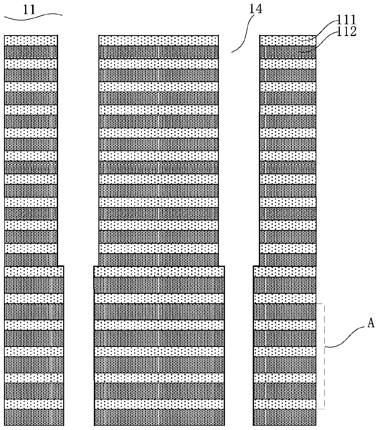
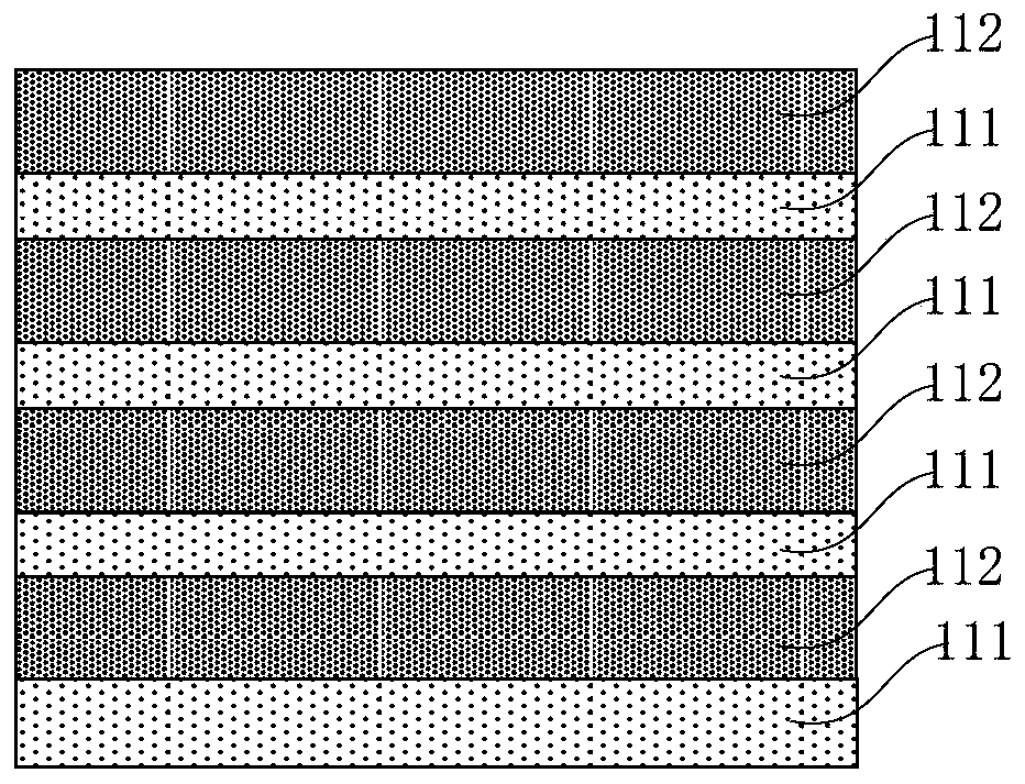
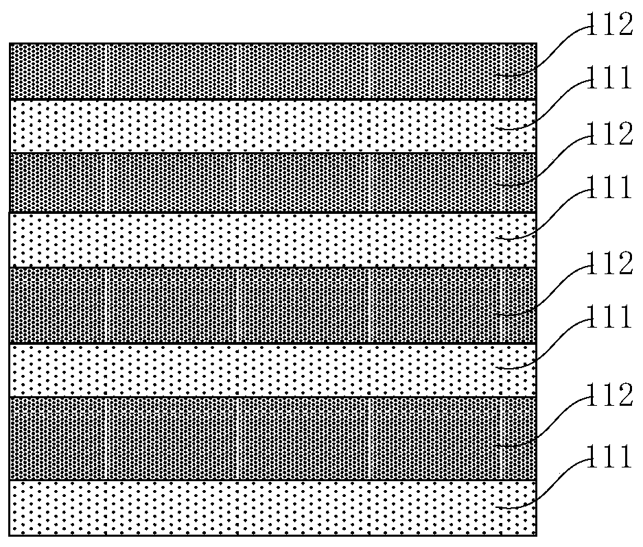
[0113] see figure 1 , the present invention provides a stacked structure 11 for a three-dimensional memory, the stacked structure 11 for a three-dimensional memory includes sacrificial layers 111 and inter-gate dielectric layers 112 alternately stacked up and down; A channel via hole 14 penetrating through the laminated structure 11 along the thickness direction of the laminated structure 11 is formed. Along the thickness direction of the laminated structure 11, the width of each part of the channel via hole 14 varies. Same; the thickness of the inter-gate dielectric layer 112 is inversely proportional to the width of the channel via hole 14 .
[0114] As an example, the laminated structure 11 can be divided into an upper part and a lower part from top to bottom along the thickness direction of the laminated structure 11, and the ratio of the upper part of the laminated structure 11 to the total thickness of the laminated structure 11 is It can be set according to actual need...
Embodiment 2
[0126] see Figure 11The present invention also provides a stacked structure 12 for a three-dimensional memory, the stacked structure 12 includes gate layers 121 and inter-gate dielectric layers 112 alternately stacked up and down; The thickness direction of the stacked structure 11 runs through the channel via hole 14 of the stacked structure 11, and along the thickness direction of the stacked structure 11, the width of each part of the channel via hole 14 is different; The thickness of the inter-gate dielectric layer 112 is inversely proportional to the width of the channel via 14 .
[0127] As an example, the laminated structure 11 can be divided into an upper part and a lower part from top to bottom along the thickness direction of the laminated structure 11, and the ratio of the upper part of the laminated structure 11 to the total thickness of the laminated structure 11 is It can be set according to actual needs; similarly, the ratio of the lower part of the laminated ...
Embodiment 3
[0139] see Figure 21 , the present invention also provides a method for preparing a three-dimensional memory, the method for preparing a three-dimensional memory includes the following steps:
[0140] 1) Provide a semiconductor substrate;
[0141] 2) forming the stacked structure as described in Embodiment 1 on the semiconductor substrate;
[0142] 3) forming an epitaxial layer at the bottom of the channel via hole;
[0143] 4) forming a functional sidewall on the sidewall of the channel via hole, and forming a channel layer on the surface of the functional sidewall and the upper surface of the epitaxial layer;
[0144] 5) forming a gate gap in the stacked structure;
[0145] 6) removing the sacrificial layer based on the gate gap to form a sacrificial gap; and
[0146] 7) Forming a gate layer in the sacrificial gap.
[0147] In step 1), see Figure 21 Step S1 in and Figure 22 , providing a semiconductor substrate 13 .
[0148] As an example, the semiconductor substr...
PUM
 Abstract
Description
Claims
Application Information


