HEMT device with sandwich grid medium structure and preparation method thereof

A gate dielectric and sandwich technology, which is applied to semiconductor devices, electrical components, circuits, etc., can solve the problems of increasing device on-resistance and gate leakage current, reducing device reliability, and increasing electron scattering. Effects of gate leakage current, reduction in electron concentration, and large threshold voltage

Active Publication Date: 2015-10-07
润新微电子(大连)有限公司
View PDF3 Cites 11 Cited by
  • Summary
  • Abstract
  • Description
  • Claims
  • Application Information

AI Technical Summary

Problems solved by technology

[0007] The present invention mainly solves the problem of the existing gate structure technical scheme formed by AlGaN barrier layer etching or fluorine ion implantation in normally-off HEMT devices, which respectively cause damage to the 2DEG channel interface used for current transport under the gate and the The increase of electron scattering in the channel leads to the increase of the on-resistance and gate leakage current of the device, and the technical problem that the reliability of the device is reduced under high temperature or high pressure working conditions. A method of partially etching the gate barrier layer and then depositing it is proposed A HEMT device with a sandwich gate dielectric structure wrapped with a fluorine ion storage layer and a preparation method thereof, under the condition of ensuring that the HEMT device has a small turn-on resistance, realize the large threshold voltage normally-off operation of the HEMT device and effectively reduce the gate of the device. Extreme leakage current, improve the breakdown voltage of the device and enhance the reliability of the device

Method used


Image

  • HEMT device with sandwich grid medium structure and preparation method thereof
  • HEMT device with sandwich grid medium structure and preparation method thereof
  • HEMT device with sandwich grid medium structure and preparation method thereof

Examples


Embodiment 1

[0058] figure 2 It is a structural schematic diagram of a HEMT device with a sandwich gate dielectric structure provided by an embodiment of the present invention. Such as figure 2 As shown, the HEMT device with the sandwich gate dielectric structure provided by the embodiment of the present invention includes:

[0059] substrate1;

[0060] a buffer layer 2 on the substrate 1;

[0061] a GaN layer 3 on the buffer layer 2;

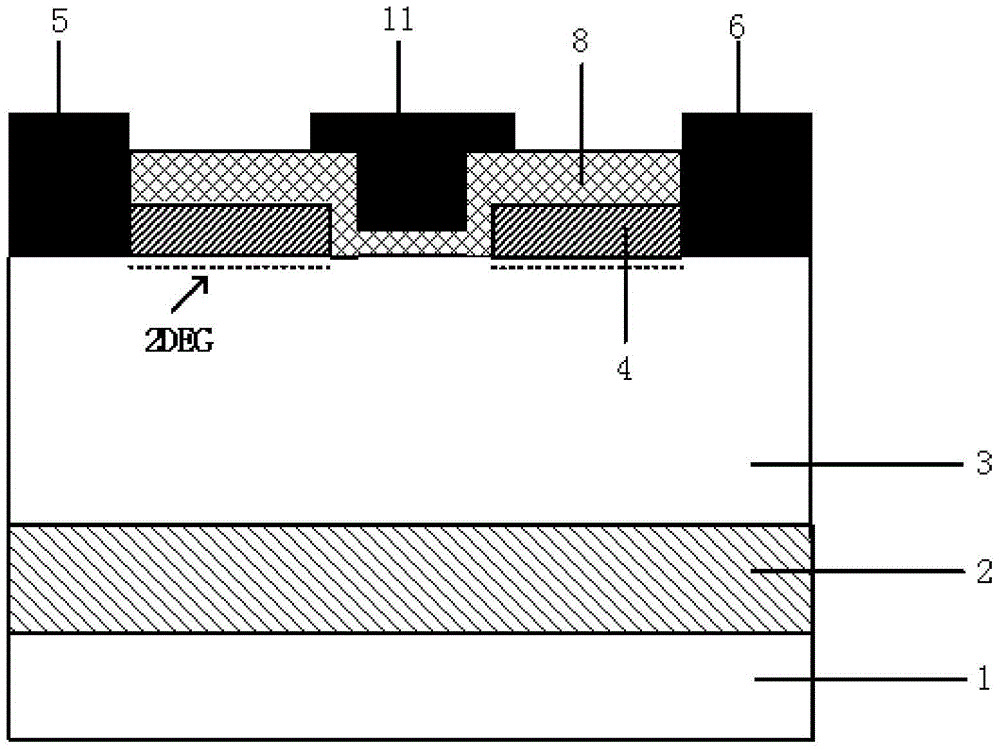
[0062] The barrier layer 4, the source electrode 5 and the drain electrode 6 located on the GaN layer 3, the barrier layer 4 has grooves on the side away from the GaN layer 3, and the barrier layer 4 has grooves on the source electrode 5 and the drain electrode 6. Between the poles 6, a heterojunction is formed between the GaN layer 3 and the barrier layer 4, and a heterojunction is formed at the interface, and the interface between the barrier layer 4 and the GaN layer 3 except the groove has a high-density 2DEG;

[0063] a passivation layer 7 locat...

Embodiment 2

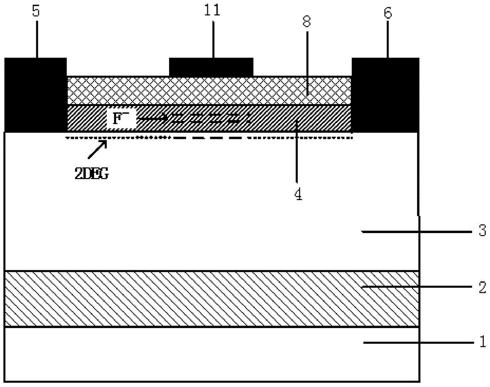
[0078] Figure 4 The flow chart of the implementation of the fabrication method of the HEMT device with the sandwich gate dielectric structure provided by the embodiment of the present invention. Such as Figure 4 As shown, the preparation method of the HEMT device with the sandwich gate dielectric structure provided by the embodiment of the present invention includes:

[0079] Step 101, forming a laminated structure sequentially composed of a substrate, a buffer layer, a GaN layer and a barrier layer.

[0080] Figure 5a It is a structural diagram corresponding to this step in the method for manufacturing a HEMT device with a sandwich gate dielectric structure provided by an embodiment of the present invention. refer to Figure 5a , forming a laminated structure consisting of a substrate 1 , a buffer layer 2 , a GaN layer 3 and a barrier layer 4 in sequence. A substrate 1 is provided; a buffer layer 2 is formed on the substrate 1 ; a GaN layer 3 is formed on the buffer l...


PUM


Abstract

The invention relates to the field of semiconductor devices, and provides a HEMT device with a sandwich grid medium structure and a preparation method thereof. The HEMT device includes a substrate, a buffer layer arranged on the substrate, a GaN layer arranged on the buffer layer, a barrier layer, a source electrode, and a drain electrode that are arranged on the GaN layer, a passivation layer arranged on the source electrode, the drain electrode, and the barrier layer except a groove, a first dielectric layer coating the groove surface and the passivation layer surface, a second dielectric layer arranged on the first dielectric layer, a third dielectric layer arranged on the second dielectric layer and the first dielectric layer except the second dielectric layer, a gate electrode in contact with the third dielectric layer, a source electrode pad in contact with the source electrode, and a drain electrode pad in contact with the drain electrode, wherein one side, far away from the GaN layer, of the barrier layer is provided with the groove, and the second dielectric layer contains fluorinion. The high-threshold voltage normally off operation of the HEMT device can be realized, and the breakdown voltage of the device can be effectively improved.

Description

technical field [0001] The invention relates to the field of semiconductor devices, in particular to a HEMT device with a sandwich gate dielectric structure and a preparation method thereof. Background technique [0002] Power switching devices are divided into normally-on (depletion) and normally-off (enhancement) types according to whether a turn-on bias is applied to the gate when the device is turned on. The normally-off power switching device is in the off state when no bias is applied to the gate electrode. Compared with the normally-on type, the normally-off type has the advantages of safer, energy-saving and simplified circuit design in practical applications. , so it has important research value and broad application market. On the other hand, the breakdown voltage is also one of the important indicators to measure the comprehensive performance of modern power devices. Various structural designs of power devices based on wide bandgap materials have been proved by e...

Claims


Application Information

Patent Timeline
Patent Type & Authority Applications(China)
IPC IPC(8): H01L29/778H01L29/06H01L29/423H01L29/66H01L21/28
CPCH01L29/0684H01L29/42364H01L29/66462H01L29/778
Inventor 黄火林
Owner 润新微电子(大连)有限公司
Why Eureka
Try Eureka