
Array substrate, display panel and method for manufacturing array substrate

A technology for array substrates and display areas, which is applied in semiconductor/solid-state device manufacturing, organic semiconductor devices, electrical components, etc., can solve problems such as cracks, poor brightness uniformity, and stretching and fracture of wiring structures, so as to reduce costs and reduce resistance Effect of pressure drop and bending stress reduction

Active Publication Date: 2019-11-08
WUHAN CHINA STAR OPTOELECTRONICS SEMICON DISPLAY TECH CO LTD
View PDF5 Cites 32 Cited by
  • Summary
  • Abstract
  • Description
  • Claims
  • Application Information

AI Technical Summary

Problems solved by technology

[0005] The purpose of the present invention is to provide an array substrate, a display panel, and a method for manufacturing the array substrate, so as to solve the problem of poor brightness uniformity of the existing organic light-emitting diode display devices and the tensile fracture of the wiring structure after repeated bending or crack technical problems

Method used


Image

  • Array substrate, display panel and method for manufacturing array substrate
  • Array substrate, display panel and method for manufacturing array substrate
  • Array substrate, display panel and method for manufacturing array substrate

Examples


Embodiment Construction

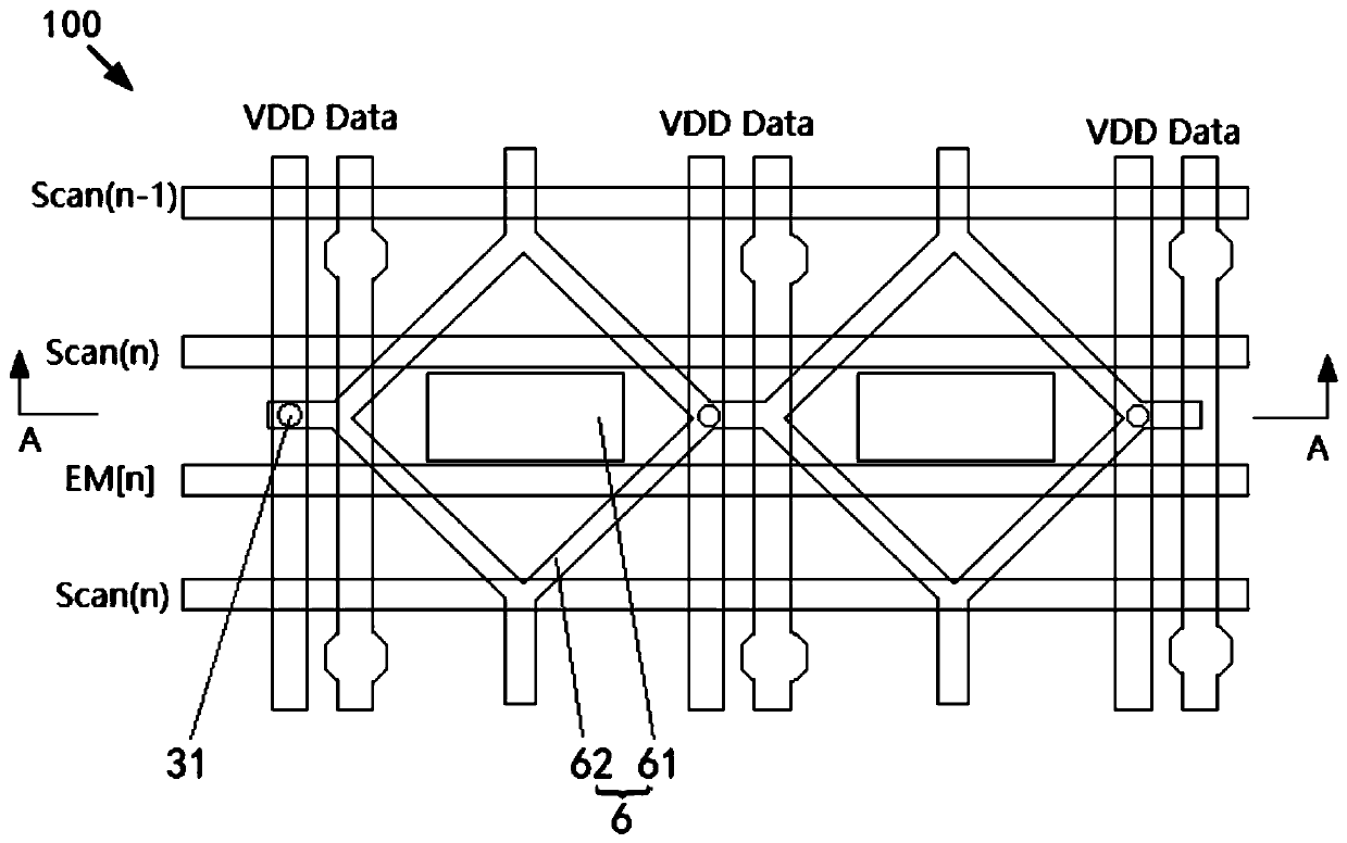
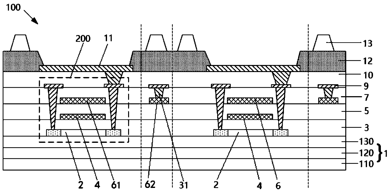
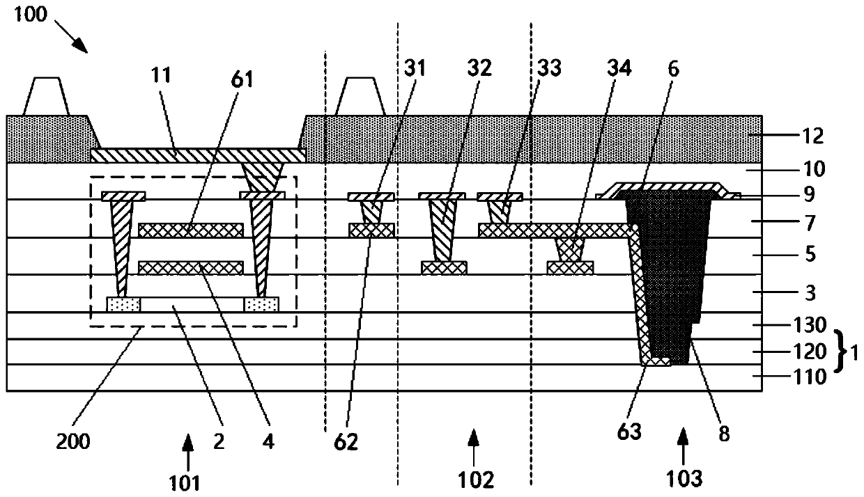
[0039] The following descriptions of the various embodiments refer to the accompanying drawings to illustrate specific embodiments in which the invention may be practiced. The directional terms mentioned in the present invention, such as [top], [bottom], [front], [back], [left], [right], [inside], [outside], [side], [horizontal], etc. , are for orientation only with reference to the attached drawings. Therefore, the directional terms used are used to illustrate and understand the present invention, but not to limit the present invention. In the figures, structurally similar elements are denoted by the same reference numerals.

[0040] The terms "first", "second", "third", etc. (if any) in the description and claims of the present invention and the above drawings are used to distinguish similar objects and not necessarily to describe a specific order or sequentially. It should be understood that the items so described are interchangeable under appropriate circumstances. Fur...


PUM

PropertyMeasurementUnit
electrical resistivityaaaaaaaaaa

Abstract

The invention discloses an array substrate, a display panel and a method for manufacturing the array substrate. The array substrate includes a substrate layer, an active layer, a first insulating layer, a first metal layer, a second insulating layer, a second metal layer, an interlayer insulating layer, an organic filling layer and a third metal layer which are disposed in a stacked manner; a mesh-shaped second metal layer is designed in the display area, and is electrically connected with a power supply voltage signal line of the third metal layer through a first via hole to form a double-layer power supply voltage trace structure in the display area. The method comprises the steps of: manufacturing a substrate layer, an active layer, a first insulating layer, a first metal layer, a second insulating layer, a second metal layer, an interlayer insulating layer, a third metal layer, a flattening layer, an anode layer, a pixel defining layer, and a support layer. By connecting the double-layer power supply voltage trace structure in the display area with the power supply voltage (VDD), the resistance voltage drop can be reduced, and the screen brightness uniformity can be improved.

Description

technical field [0001] The present invention relates to the field of display technology, in particular to an array substrate, a display panel and a method for manufacturing the array substrate. Background technique [0002] Due to the advantages of light weight, self-illumination, wide viewing angle, low driving voltage, high luminous efficiency, low power consumption, and fast response speed of organic light emitting diode display devices (Organic Light Emitting Display, OLED), the application range is more and more extensive, especially flexible The OLED display device has the characteristics of being bendable and easy to carry, and has become a main field of research and development in the field of display technology. [0003] At present, the bendable display screen has attracted much attention, but the service life of the display screen is seriously affected due to the tensile fracture or cracks in the wiring structure after repeated bending. At the same time, high-end ...

Claims


Application Information

Patent Timeline
Patent Type & Authority Applications(China)
IPC IPC(8): H01L27/32H01L51/56H10K99/00
CPCH10K59/123H10K59/1213H10K59/1315H10K59/1201H10K71/421H10K59/131H10K10/482H10K59/124H10K71/00H10K77/111H10K2102/311
Inventor 陈诚余赟
Owner WUHAN CHINA STAR OPTOELECTRONICS SEMICON DISPLAY TECH CO LTD
Learn More