A si-apd photodetector based on fractal nanowire surface structure and its preparation method

A photoelectric detector and surface structure technology, applied in the field of photoelectric detection, can solve the problems of low reflectivity, low transmittance, etc., achieve strong optical absorption characteristics, simple preparation process, and high efficiency

Active Publication Date: 2021-07-30
重庆连芯智能科技研究院有限公司
View PDF7 Cites 0 Cited by
  • Summary
  • Abstract
  • Description
  • Claims
  • Application Information

AI Technical Summary

Problems solved by technology

The surface structure of nanowires (nanoholes) has extremely strong absorption for specific wavelengths, which can achieve low reflectivity and low transmittance, but only for a single wavelength

Method used


Image

  • A si-apd photodetector based on fractal nanowire surface structure and its preparation method
  • A si-apd photodetector based on fractal nanowire surface structure and its preparation method

Examples


Embodiment Construction

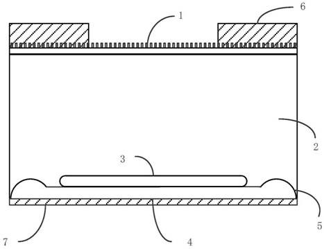
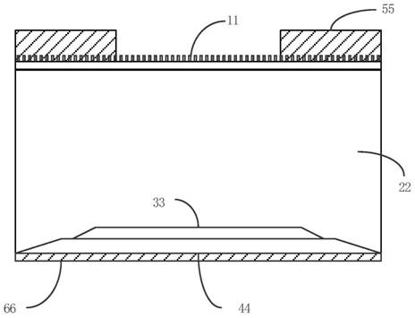
[0038] In order to make the purpose, technical solutions and advantages of the embodiments of the present invention clearer, the technical solutions in the embodiments of the present invention will be clearly and completely described below in conjunction with the drawings in the embodiments of the present invention. Obviously, the described embodiments are only It is a part of embodiments of the present invention, but not all embodiments. The components of the embodiments of the invention generally described and illustrated in the figures herein may be arranged and designed in a variety of different configurations. Accordingly, the following detailed description of the embodiments of the invention provided in the accompanying drawings is not intended to limit the scope of the claimed invention, but merely represents selected embodiments of the invention. Based on the embodiments of the present invention, all other embodiments obtained by those skilled in the art without making...


PUM

PropertyMeasurementUnit
lengthaaaaaaaaaa
reflectanceaaaaaaaaaa

Abstract

The invention discloses a Si‑APD photodetector based on a fractal nanowire surface structure and a preparation method thereof, comprising: a P+ area of ​​the light-incoming layer with a fractal nano-wire surface structure, and a local area below the P+ area of ​​the light-incoming layer with a fractal nanowire surface structure The π region of the intrinsic absorption layer, the P region of the avalanche multiplication layer located under the π region of the intrinsic absorption layer, the N+ region of the electrode contact layer located below the P region of the avalanche multiplication layer, and the protection rings located under the two sides of the π region of the intrinsic absorption layer are N region, the upper end electrode arranged on the upper surface of the P+ region of the fractal nanowire surface structure light-incoming layer, and the lower electrode of the electrode contact layer N+ region and the lower surface of the N-region; the P+ region of the fractal nanowire surface structure light-incoming layer has a random fractal Surface structure of distributed vertical silicon nanowires. The invention solves the problems of low responsivity of the traditional Si-APD photodetector and almost no response in the near-infrared band, and can enhance the quantum efficiency of visible light detection and extend the response band to the near-infrared band.

Description

technical field [0001] The invention belongs to the technical field of photoelectric detection, and relates to a photoelectric detection device structure, in particular to a Si-APD photodetector based on a fractal nanowire surface structure and a preparation method thereof. Background technique [0002] As an important part of optical fiber communication system, infrared imaging system, laser warning system and laser ranging system, photoelectric detectors have been widely used in civilian and military applications. [0003] APD is a photodetector with internal gain capability and high sensitivity, which is widely used in ultra-high-speed optical communication, signal processing, measurement and sensing systems. APD is a photodetector widely used in modern high-bit-rate optical communication systems. It has been widely used in weak light field measurement, photon Counting and other related fields. It is mainly used in communication, aviation, aerospace, navigation, medical...

Claims


Application Information

Patent Timeline
Patent Type & Authority Patents(China)
IPC IPC(8): H01L31/107H01L31/028H01L31/0236H01L31/18
CPCH01L31/02363H01L31/028H01L31/107H01L31/1804Y02P70/50
Inventor 杨奇龙马晓燠饶学军汪韬盛良睿
Owner 重庆连芯智能科技研究院有限公司
Why Eureka
Try Eureka