Si-apd photodetector based on micro-nano structure and its preparation method

A micro-nano structure and photodetector technology, applied in the field of photodetection, can solve the problems of high price, low responsivity, and large forbidden band width of silicon materials, and achieves improved responsivity and quantum efficiency, good processing repeatability, and preparation. Simple process effect

Inactive Publication Date: 2016-09-14
UNIV OF ELECTRONICS SCI & TECH OF CHINA
View PDF5 Cites 0 Cited by
  • Summary
  • Abstract
  • Description
  • Claims
  • Application Information

AI Technical Summary

Problems solved by technology

[0004] The traditional silicon-based avalanche photodiode (Si-APD) has a high responsivity in the wavelength range of 200 nm to 900 nm, but the band gap of silicon material is large (1.12 eV), so the traditional Si-APD is not sensitive to wavelengths greater than 1000 nm. The light responsivity is very low, and generally cannot be used for light detection in the infrared band
Although other semiconductor materials such as Ge and InGaAs can detect light in the infrared band, these materials are expensive, have poor thermodynamic properties, low signal-to-noise ratio, and the device preparation process is not compatible with the existing mature silicon process.

Method used


Image

  • Si-apd photodetector based on micro-nano structure and its preparation method
  • Si-apd photodetector based on micro-nano structure and its preparation method

Examples


Embodiment Construction

[0037] The present invention will be further described below in conjunction with the accompanying drawings and specific embodiments.

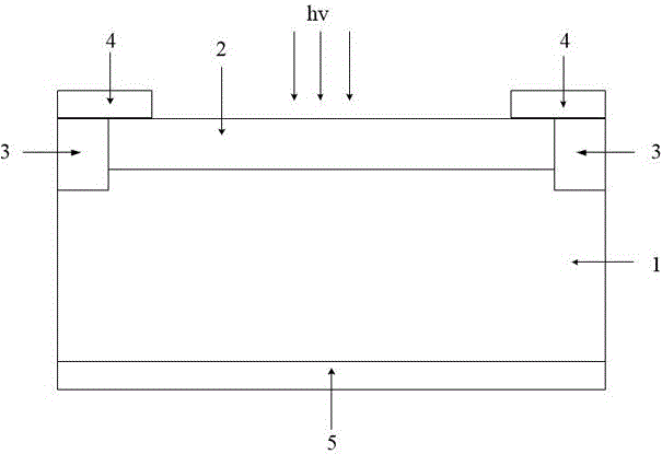
[0038] like figure 1As shown, it includes a P-type Si substrate 1 , an N+ region 2 , an N region 3 , an upper end electrode 4 and a lower end electrode 5 . P-type Si substrate 1 can adopt high-resistance Si single wafer; N region 3 can adopt phosphorus diffusion or ion implantation; micro-nanostructure silicon layer N+ region 2 can be formed on the N+ region by phosphorus diffusion doping or ion implantation. printed and etched. The novel Si-APD photodetector fabricated in this way has the characteristics of high responsivity and near-infrared wide spectral response with micro-nano structured silicon layer and guard ring.

[0039] A kind of Si-APD photodetector based on micro-nano structure, specifically comprises the following steps:

[0040] Prepare the surface clean and dry silicon single wafer substrate material;

[0041] Grind and ...


PUM


Abstract

The present invention discloses a Si-APD photoelectric detector based on a micro-nano structure and a preparation method thereof, belonging to the photoelectric detection technology field. The Si-APD photoelectric detector based on the micro-nano structure comprises a P-type Si substrate (1), a micro-nano structure silicon layer N+ area (2) located above the center of the P-type Si substrate (1), protection annular areas, namely N areas (3) located above the two sides of the P-type Si substrate (1), upper-end electrodes (4) arranged on the upper surfaces of the micro-nano structure silicon layer N+ area (2) and the N areas, and a lower-end electrode (5) located on the lower surface of the P-type Si substrate (1), wherein the depth of the micro-nano structure silicon layer N+ area (2) is less than the depths of the protection annular areas, namely the N areas (3). The Si-APD photoelectric detector based on the micro-nano structure and the preparation method thereof of the present invention solve the problems that the conventional Si-APD photoelectric detector is lower in responsivity, can not respond a near-infrared band, etc., enables the response wave band to be expanded to the near-infrared band, and is higher in responsivity.

Description

technical field [0001] The invention belongs to the technical field of photoelectric detection, and relates to the structure of a photoelectric detection device, in particular to a Si-APD photodetector based on a micro-nano structure and a preparation method thereof. Background technique [0002] As an important part of optical fiber communication system, infrared imaging system, laser warning system and laser ranging system, photoelectric detectors have been widely used in civilian and military applications. APD is a photodetector with internal gain capability and high sensitivity, which is widely used in ultra-high-speed optical communication, signal processing, measurement and sensing systems. APD is a photodetector widely used in modern high-bit-rate optical communication systems. It has been widely used in weak light field measurement, photon Counting and other related fields. Because the APD photodetector has the characteristics of higher internal gain and higher det...

Claims


Application Information

Patent Timeline
Patent Type & Authority Patents(China)
IPC IPC(8): H01L31/028H01L31/0352H01L31/101H01L31/18
CPCH01L31/028H01L31/035209H01L31/103H01L31/1804Y02P70/50
Inventor 李伟吴程呈渠叶君钟豪蒋亚东
Owner UNIV OF ELECTRONICS SCI & TECH OF CHINA
Why Eureka
Try Eureka