Artificial dielectric surface based on tight-coupling double-sided patch structure

A dielectric and tight-coupling technology, applied in the direction of electrical components, antennas, etc., can solve problems such as difficult to meet, high relative permittivity, and inability to meet the needs of flexible regulation of electromagnetic waves, and achieve the effect of flexible regulation and wide regulation range

Inactive Publication Date: 2019-11-15
SUZHOU UNIV
View PDF9 Cites 0 Cited by
  • Summary
  • Abstract
  • Description
  • Claims
  • Application Information

AI Technical Summary

Problems solved by technology

However, the adjustable range of the relative permittivity of the artificial dielectric surface based on the I-shaped and square-ring unit structures is narrow, which cannot meet the ne

Method used


Image

  • Artificial dielectric surface based on tight-coupling double-sided patch structure
  • Artificial dielectric surface based on tight-coupling double-sided patch structure
  • Artificial dielectric surface based on tight-coupling double-sided patch structure

Examples


Embodiment 1

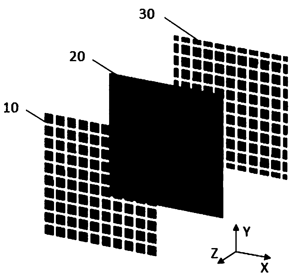
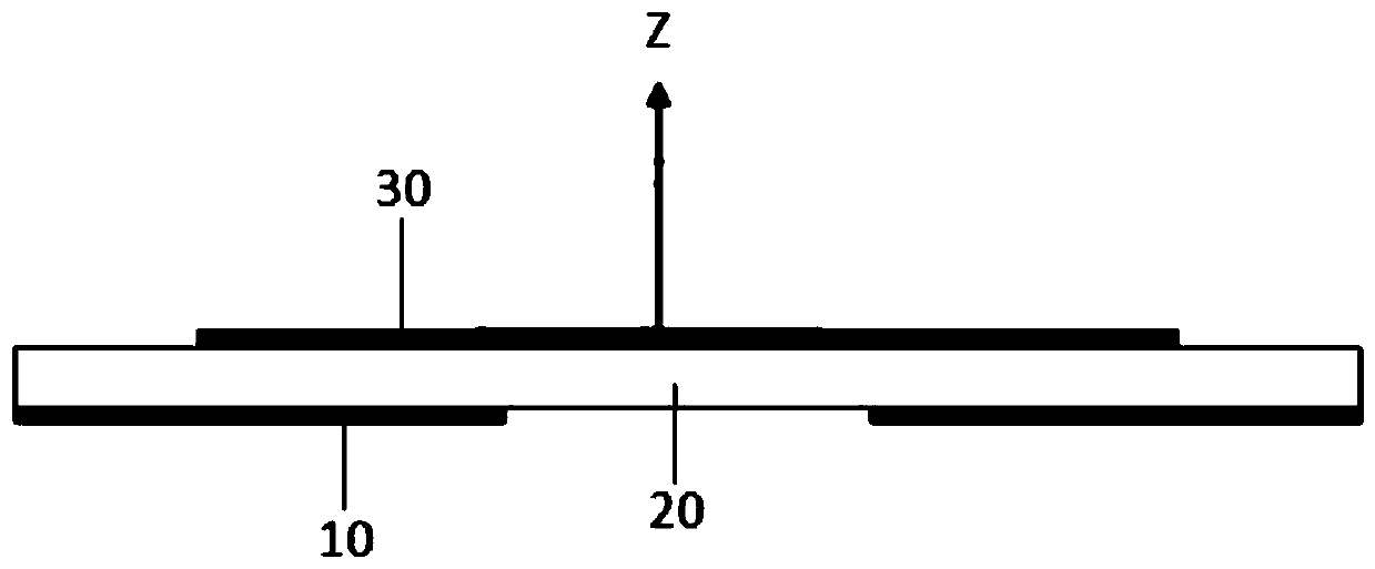
[0026] Such as Figure 1-5 As shown, it is an artificial dielectric surface based on a tightly coupled double-sided patch structure in Embodiment 1 of the present invention. The artificial dielectric surface based on a tightly coupled double-sided patch structure includes an upper metal layer 10 and a dielectric layer arranged in sequence from top to bottom. Substrate 20 and underlying metal layer 30 .

[0027] Both the upper metal layer 10 and the lower metal layer 30 are formed by a periodic array of square patches of equal size, and the square patches of the upper metal layer 10 and the lower metal layer 30 have relative offsets in the X and Y directions.

[0028] Such as Figure 2-5 As shown, it is the periodic unit of the artificial dielectric surface based on the tightly coupled double-sided patch structure in this embodiment. In one periodic unit, it includes a complete square patch of the upper metal layer 10 and four square patches of the lower metal layer 30. One-t...

Embodiment 2

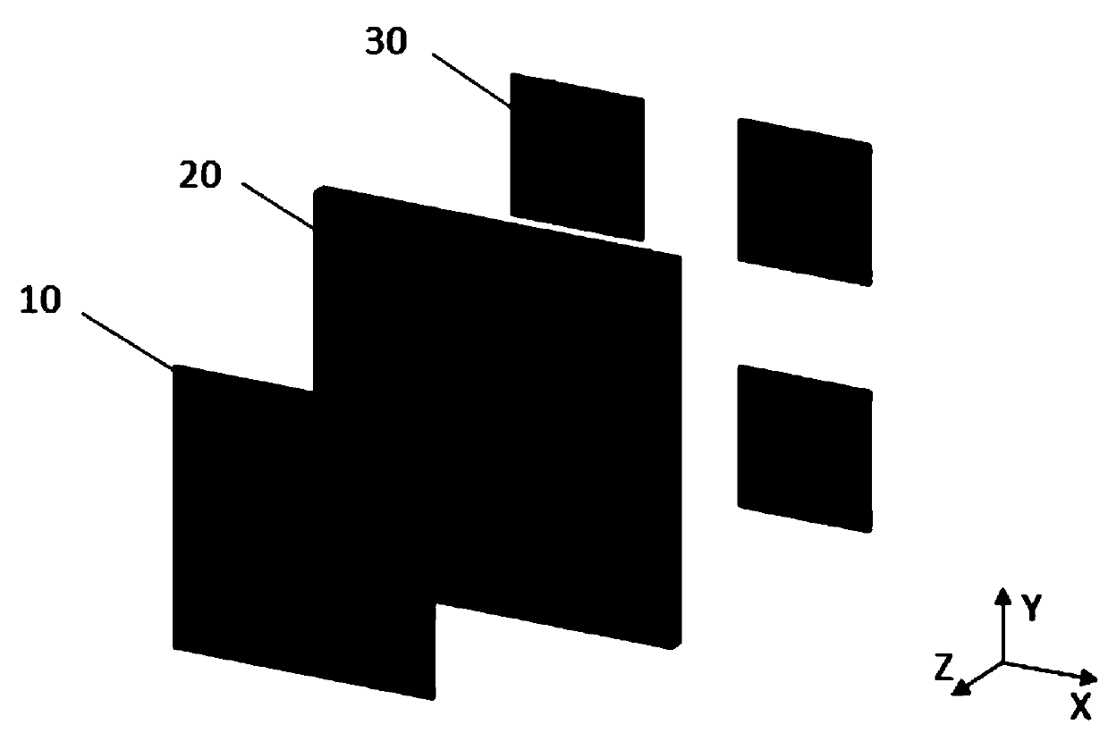
[0032] Such as Figure 7 As shown, it is the artificial dielectric surface based on the tightly coupled double-sided patch structure in this embodiment, which includes a plurality of artificial dielectric surface units, and the plurality of artificial dielectric surface units are arranged periodically along the Z direction, that is, the direction perpendicular to the artificial dielectric surface unit As a result, the artificial dielectric surface unit in this embodiment has the same structure as the artificial dielectric surface unit in Embodiment 1, specifically as Figure 1-5 shown.

[0033] Specifically, the artificial dielectric surface in this embodiment includes an upper metal layer 10, a dielectric substrate 20, and a lower metal layer 30 arranged in sequence from top to bottom, and the upper metal layer 10 and the lower metal layer 30 are made of square patches of equal size Formed in a periodic array, the square patches of the upper metal layer 10 and the lower meta...


PUM

PropertyMeasurementUnit
Thicknessaaaaaaaaaa
Thicknessaaaaaaaaaa
Thicknessaaaaaaaaaa

Abstract

The invention discloses an artificial dielectric surface based on a tight-coupling double-sided patch structure. The artificial dielectric surface based on a tight-coupling double-sided patch structure includes an upper metal layer, a dielectric substrate and a lower metal layer arranged in turn from top to bottom. The upper metal layer and the lower metal layer are formed by periodically arrayingsquare patches of equal size, and the square patches of the upper metal layer and the lower metal layer have a relative offset in both the X and Y directions. The artificial dielectric surface basedon a tight-coupling double-sided patch structure in the invention has a wide adjustment range and a high upper limit value of the equivalent relative dielectric constant, which can meet the need for flexible regulation of electromagnetic wave in the existing high-performance application occasions. The artificial dielectric surface presented by the invention has high unit resonance frequency, whichcan meet the requirement for a higher relative dielectric constant at higher microwave frequency such as above 20GHz.

Description

technical field [0001] The invention relates to the technical field of artificial dielectric surfaces, in particular to an artificial dielectric surface based on a tightly coupled double-sided patch structure. Background technique [0002] The artificial dielectric surface is an artificial structure with equivalent dielectric properties that is periodically arranged with sub-wavelength artificial structures. In recent years, artificial dielectric surfaces have been widely used in microwave and antenna engineering, such as reducing the size of microwave devices, increasing the directivity of antennas, and realizing antenna beam steering. In the application of lens antennas, artificial dielectric surfaces have obvious advantages in terms of refractive index, impedance, and polarization. For example, in the gradient index (GRIN) metamaterial lens antenna, the square annular artificial dielectric surface is used to increase the bandwidth and achieve dual polarization; in the IM...

Claims


Application Information

Patent Timeline
IPC IPC(8): H01Q15/00
CPCH01Q15/00
Inventor 杨歆汨孙达
Owner SUZHOU UNIV
Why Eureka
Try Eureka