An artificial dielectric surface based on a coplanar bidirectional interdigitated patch structure

A dielectric and interdigital technology, applied in the field of artificial dielectric surfaces based on coplanar bidirectional interdigital patch structure, can solve the problems of high processing cost, narrow adjustable range of relative dielectric constant, low resonance frequency, etc. reduced effect

Active Publication Date: 2021-04-06
SUZHOU UNIV
View PDF9 Cites 0 Cited by
  • Summary
  • Abstract
  • Description
  • Claims
  • Application Information

AI Technical Summary

Problems solved by technology

However, the adjustable range of the relative permittivity of the artificial dielectric surface based on the I-shaped and square-ring unit structures is narrow, which cannot meet the needs of flexible control of electromagnetic waves in existing high-performance applications; Microwave frequency such as above 20GHz to achieve higher relative permittivity requirements
[0004] In addition, some new artificial dielectric surfaces, such as the artificial dielectric surface with tightly coupled double-sided patch structure or double-sided positive interdigitated strip structure as the basic periodic unit, have similar working principles to I-shaped artificial dielectric and square-ring artificial dielectric surface. , although they can achieve a higher relative permittivity and a wider relative permittivity adjustment range in the higher microwave frequency band, each unit needs to etch a double-sided metal pattern through the PCB process, and the processing cost is relatively high

Method used


Image

  • An artificial dielectric surface based on a coplanar bidirectional interdigitated patch structure
  • An artificial dielectric surface based on a coplanar bidirectional interdigitated patch structure
  • An artificial dielectric surface based on a coplanar bidirectional interdigitated patch structure

Examples


Embodiment 1

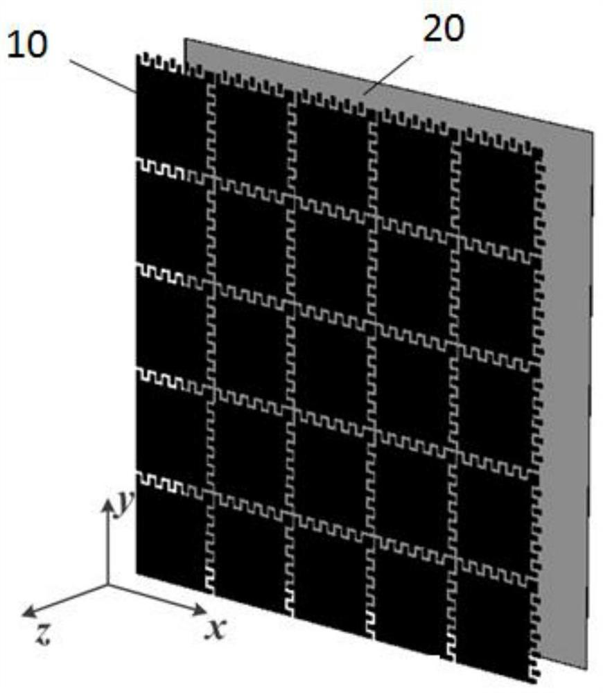
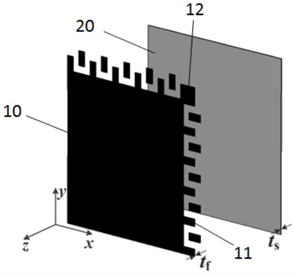
[0030] Such as Figure 1-3 As shown, it is the artificial dielectric surface based on the coplanar bidirectional interdigitated patch structure in Embodiment 1 of the present invention. The artificial dielectric surface based on the coplanar bidirectional interdigitated patch structure includes a body, and the body includes sequentially arranged from top to bottom Metal cladding and dielectric substrate 20 . The entire artificial dielectric surface is a two-dimensional periodic surface.

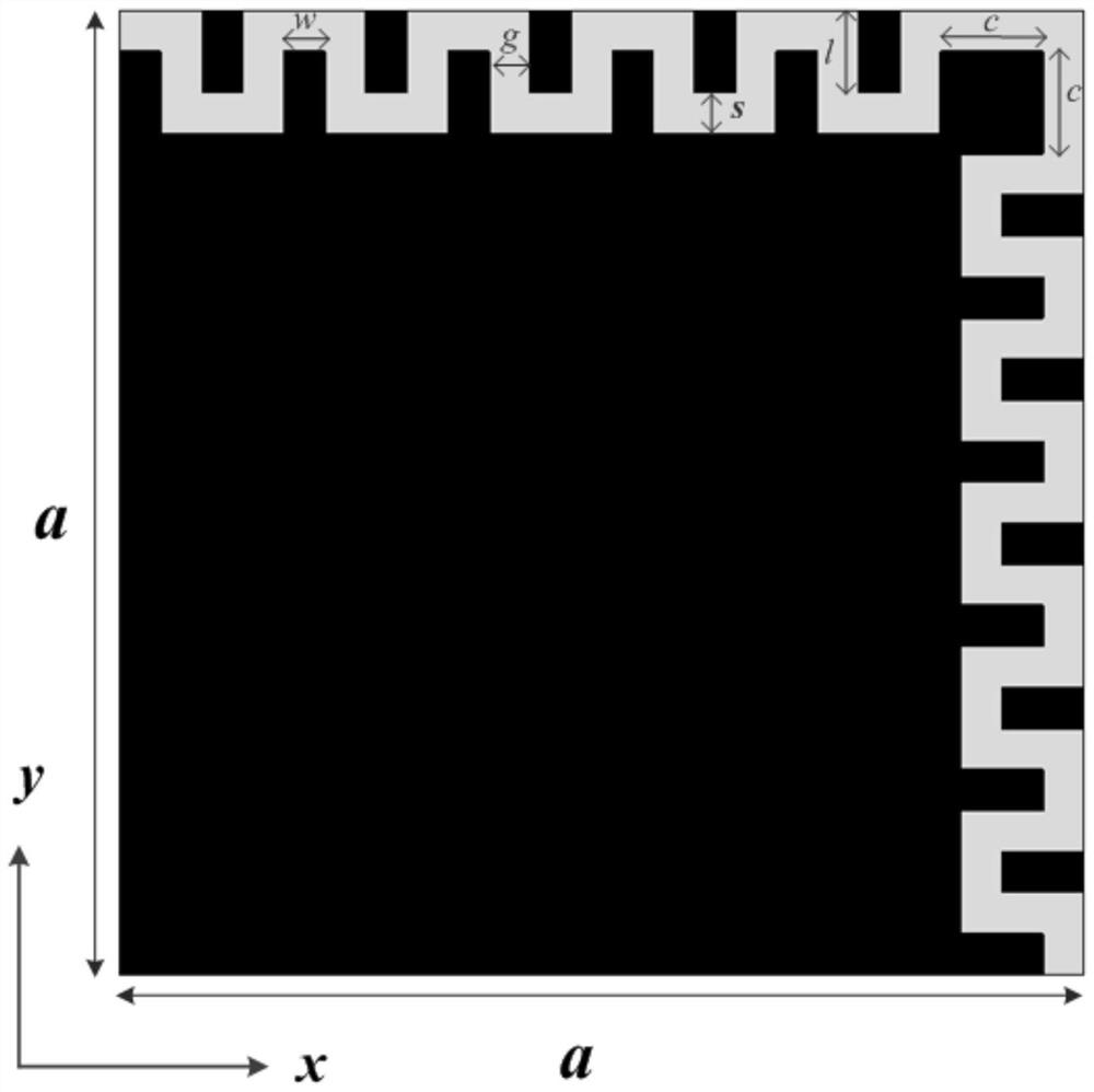
[0031] Specifically, the metal cladding is formed by a 10-period array of square metal patches of equal size, such as Figure 2-3 As shown, it is the artificial dielectric surface unit based on the coplanar bidirectional interdigitated patch structure in the embodiment of the present invention, each unit protects a square metal patch 10, and the edges of the four sides of the square metal patch 10 are provided with periodic There are permanent protrusions 11, a groove is formed between two ...

Embodiment 2

[0037] Such as Figure 5 Shown is the artificial dielectric surface based on the coplanar bidirectional interdigitated patch structure in this embodiment, which includes a plurality of bodies, and the plurality of bodies are periodically arranged along the Z direction. The specific structure of each ontology is as Figure 1-3 shown.

[0038] Specifically, the body in this embodiment includes a metal coating and a dielectric substrate 20 arranged in sequence from top to bottom.

[0039] Specifically, the metal cladding is formed by a periodic array of 10 square metal patches of equal size. The edges of the four sides of the square metal patch 10 are provided with periodic protrusions 11, and concave holes are formed between two adjacent protrusions 11. The grooves, the protrusions 11 on two adjacent square metal patches 10 are inserted into each other's grooves, and there is a gap with the inner wall of the grooves.

[0040] In this embodiment, both the protrusion 11 and the...


PUM

PropertyMeasurementUnit
thicknessaaaaaaaaaa
thicknessaaaaaaaaaa
lengthaaaaaaaaaa

Abstract

The invention discloses an artificial dielectric surface based on a coplanar bidirectional interdigitated patch structure, which includes a body, the body includes a metal coating and a dielectric substrate arranged in sequence from top to bottom, and the metal coating consists of squares of equal size The metal patches are formed in a periodic array, and the edges of the four sides of the square metal patch are provided with periodic protrusions, and grooves are formed between two adjacent protrusions, and the protrusions on the adjacent two square metal patches are mutually connected. are inserted into the grooves of each other, and have a gap with the inner wall of the grooves. The equivalent relative permittivity of the artificial dielectric surface based on the coplanar bidirectional interdigitated patch structure of the present invention has a wide adjustment range and a high upper limit, which can meet the needs of flexible control of electromagnetic waves in existing high-performance applications , which can meet the requirement of high relative permittivity at higher microwave frequencies such as above 20 GHz. It only has a single-sided metal pattern, and the processing cost is significantly reduced.

Description

technical field [0001] The invention relates to the technical field of artificial dielectric surfaces, in particular to an artificial dielectric surface based on a coplanar bidirectional interdigitated patch structure. Background technique [0002] The artificial dielectric surface is an artificial structure with equivalent dielectric properties that is periodically arranged with sub-wavelength artificial structures. In recent years, artificial dielectric surfaces have been widely used in microwave and antenna engineering, such as reducing the size of microwave devices, increasing the directivity of antennas, and realizing antenna beam steering. In the application of lens antennas, artificial dielectric surfaces have obvious advantages in terms of refractive index, impedance, and polarization. For example, in the gradient index (GRIN) metamaterial lens antenna, the square annular artificial dielectric surface is used to increase the bandwidth and achieve dual polarization; ...

Claims


Application Information

Patent Timeline
Patent Type & Authority Patents(China)
IPC IPC(8): H01Q15/00
CPCH01Q15/00
Inventor 杨歆汨李烨朱立宇
Owner SUZHOU UNIV
Why Eureka
Try Eureka