Microhole filling paste for circuit board, preparation method and application thereof

A technology of circuit boards and micro-holes, which is applied in the manufacture of printed circuits, circuits, printed circuits, etc., can solve problems affecting the development of circuit boards, and achieve the effects of dense holes, good electrical conductivity, and improved toughness

Active Publication Date: 2022-04-12
SEMITEL ELECTRONICS
View PDF8 Cites 0 Cited by
  • Summary
  • Abstract
  • Description
  • Claims
  • Application Information

AI Technical Summary

Problems solved by technology

With the development of science and technology, the function requirements of mobile phones are becoming more and more powerful. In the application, it is found that the LCP flexible board has developed into a 5-layer board or even a 7-layer board. The electroplating process cannot reach the filling of blind holes exceeding 0.2mm, which seriously affects the development of the circuit board industry.

Method used


Image

  • Microhole filling paste for circuit board, preparation method and application thereof
  • Microhole filling paste for circuit board, preparation method and application thereof
  • Microhole filling paste for circuit board, preparation method and application thereof

Examples


Embodiment Construction

[0028] The preferred embodiments of the present invention will be described in detail below in conjunction with the accompanying drawings, so that the advantages and features of the present invention can be more easily understood by those skilled in the art, so as to define the protection scope of the present invention more clearly.

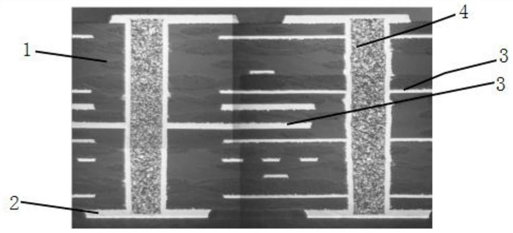
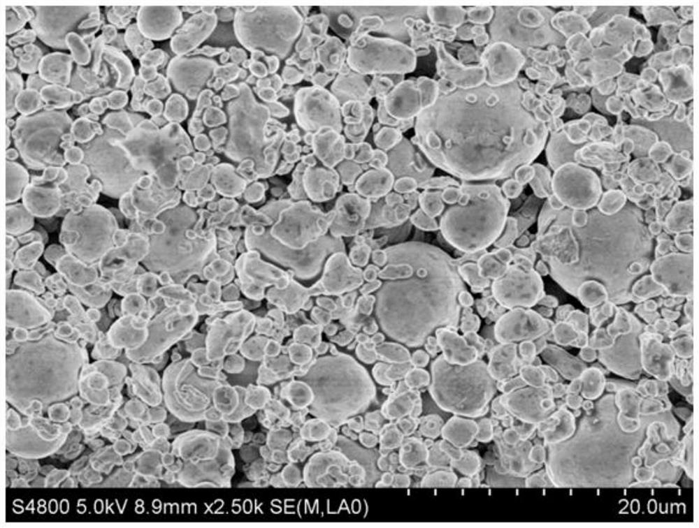
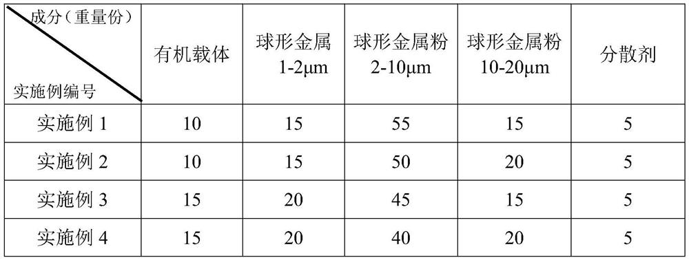
[0029] A micropore filling slurry for circuit boards, comprising the following raw materials in parts by weight: 5-20 parts of organic carrier, 15-30 parts of spherical metal powder with a particle size of 1-2 μm, and spherical metal powder with a particle size of 2-10 μm. 30-60 parts of powder, 10-20 parts of spherical metal powder with a particle size of 10-20 μm and 1-5 parts of dispersant.

[0030] Wherein, the organic vehicle includes the following raw materials in parts by weight: 70-90 parts of epoxy resin, 1-5 parts of curing agent, 5-10 parts of DBE solvent, 5-10 parts of liquid crystal polymer material, 1-5 parts of curing accelerator 1...


PUM

PropertyMeasurementUnit
particle diameteraaaaaaaaaa

Abstract

The invention discloses a micropore filling slurry for a circuit board, which comprises the following raw materials in parts by weight: 5-20 parts of an organic carrier, 15-30 parts of spherical metal powder with a particle diameter of 1-2 μm, and a particle diameter of 2-2 μm. 30-60 parts of spherical metal powder of 10 μm, 10-20 parts of spherical metal powder with particle size of 10-20 μm and 1-5 parts of dispersant. The invention also discloses a preparation method and application of the micropore filling slurry for circuit boards. The slurry of the invention has the advantages of high electrical conductivity and high thermal shock resistance, is suitable for micropore filling, and has excellent comprehensive performance.

Description

technical field [0001] The invention relates to a conductive paste for circuit boards, in particular to a micropore filling paste for circuit boards and a preparation method thereof, which is applied to filling holes in circuit boards such as LCP soft boards, PCB circuit boards and PI soft boards, especially in LCP soft board has obvious advantages. Background technique [0002] With the ultimate pursuit of miniaturization in mobile phones and wearable products, embedding components in multilayer circuit boards is a long-term development trend of industry technology. In the 5G era, the number of components in antennas and RF front-ends will increase dramatically, and the demand for embedding and packaging millimeter-wave circuits into multilayer circuit boards is increasingly urgent. The multi-layer structure of LCP can realize the modular packaging of high-frequency circuits such as antennas and RF front-ends, and its functional attributes and product value have been quali...

Claims


Application Information

Patent Timeline
Patent Type & Authority Patents(China)
IPC IPC(8): H05K1/09H05K3/00H01B1/22H01B13/00
CPCH05K1/092H05K3/0094H01B1/22H01B13/00H05K2201/09563
Inventor 董福兴戴剑王凯袁生红仇利民崔海周
Owner SEMITEL ELECTRONICS
Why Eureka
Try Eureka