Full CMOS reference circuit

A reference circuit and reference voltage technology, applied in the direction of adjusting electrical variables, control/regulation systems, instruments, etc., can solve problems such as non-subordination

Pending Publication Date: 2019-11-26
丹阳恒芯电子有限公司
View PDF4 Cites 0 Cited by
  • Summary
  • Abstract
  • Description
  • Claims
  • Application Information

AI Technical Summary

Problems solved by technology

The traditional method can be designed with a bandgap reference circuit, but its power ...

Method used


Image

  • Full CMOS reference circuit

Examples


Embodiment Construction

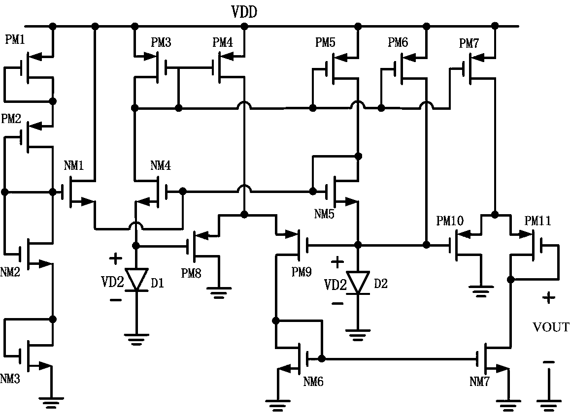
[0011] combine figure 1 As shown, in the following embodiments, the full CMOS reference circuit at least includes: a start-up circuit for starting the reference circuit; a core reference circuit adopts a self-bias structure, and the accuracy of the reference voltage generated is It is also very high and less affected by temperature. Since no resistors are used in the entire circuit, the overall circuit area is also very small.

[0012] The start-up circuit is composed of a first PMOS transistor PM1, a second PMOS transistor PM2, a first NMOS transistor NM1, a second NMOS transistor NM2 and a third NMOS transistor NM3; the PM1 transistor, PM2 transistor, NM2 transistor and NM3 transistor are all diodes In the connection method, when the power supply voltage is applied to the circuit and the core reference circuit is not started, the NM1 tube is turned on, the gate voltage of the NM4 tube is pulled up, the NM4 tube is turned on, and the core reference circuit is started; when th...


PUM


Abstract

The invention discloses a full CMOS reference circuit, comprising a starting circuit used for starting a reference circuit, and a core reference circuit adopting a self-bias structure. According to the full CMOS reference circuit, the precision of the generated reference voltage is very high, the influence of the temperature is small, and the area of the whole circuit is very small because no resistor is adopted in the whole circuit.

Description

technical field [0001] The invention relates to the field of reference voltage circuits, in particular to an all-CMOS reference circuit. Background technique [0002] In the Internet of Things, EEPROM and most wireless communication applications, the relevant receiving circuits or transmitting circuits require low power consumption, so a reference circuit that can generate low power consumption is very critical and necessary for the entire application . As an important part of the analog circuit, the reference circuit generally needs to work normally in a wide temperature range. Therefore, not only low power consumption is required, but also stable performance and good temperature characteristics are required. The traditional method can be designed with a bandgap reference circuit, but its power consumption is at the microwatt level, which does not belong to the low-power design category. Contents of the invention [0003] In order to overcome the above-mentioned problem...

Claims


Application Information

Patent Timeline
IPC IPC(8): G05F1/567
CPCG05F1/567
Inventor 陈磊
Owner 丹阳恒芯电子有限公司
Why Eureka
Try Eureka