Touch device

A touch device and touch electrode technology are applied in the fields of instruments, electrical digital data processing, and data processing input/output processes to reduce noise problems and improve sensitivity and accuracy.

Active Publication Date: 2019-11-26
AU OPTRONICS CORP
View PDF6 Cites 0 Cited by
  • Summary
  • Abstract
  • Description
  • Claims
  • Application Information

AI Technical Summary

Problems solved by technology

The display medium layer is located on the array substrate

Method used


Image

  • Touch device
  • Touch device
  • Touch device

Examples


Embodiment Construction

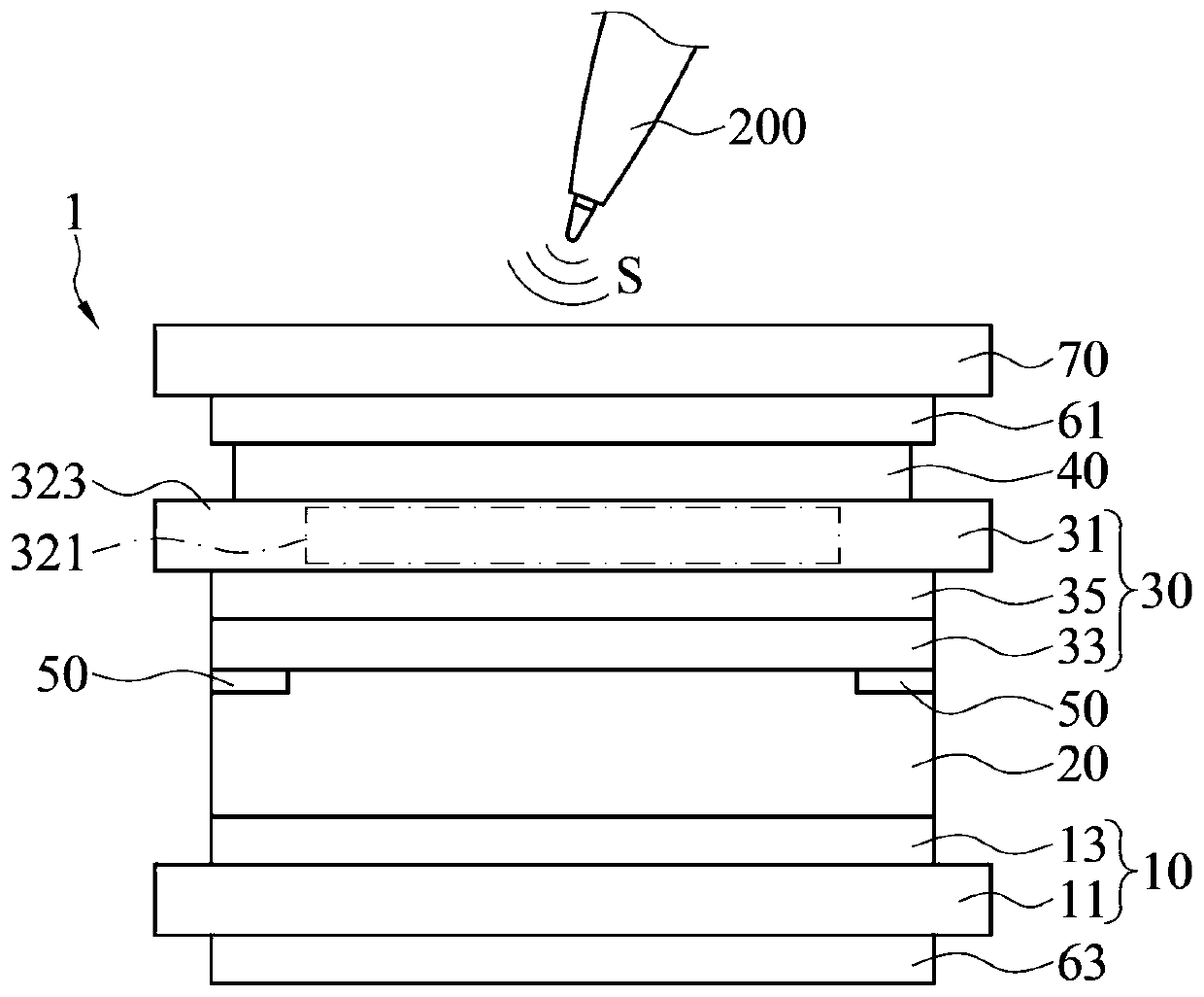
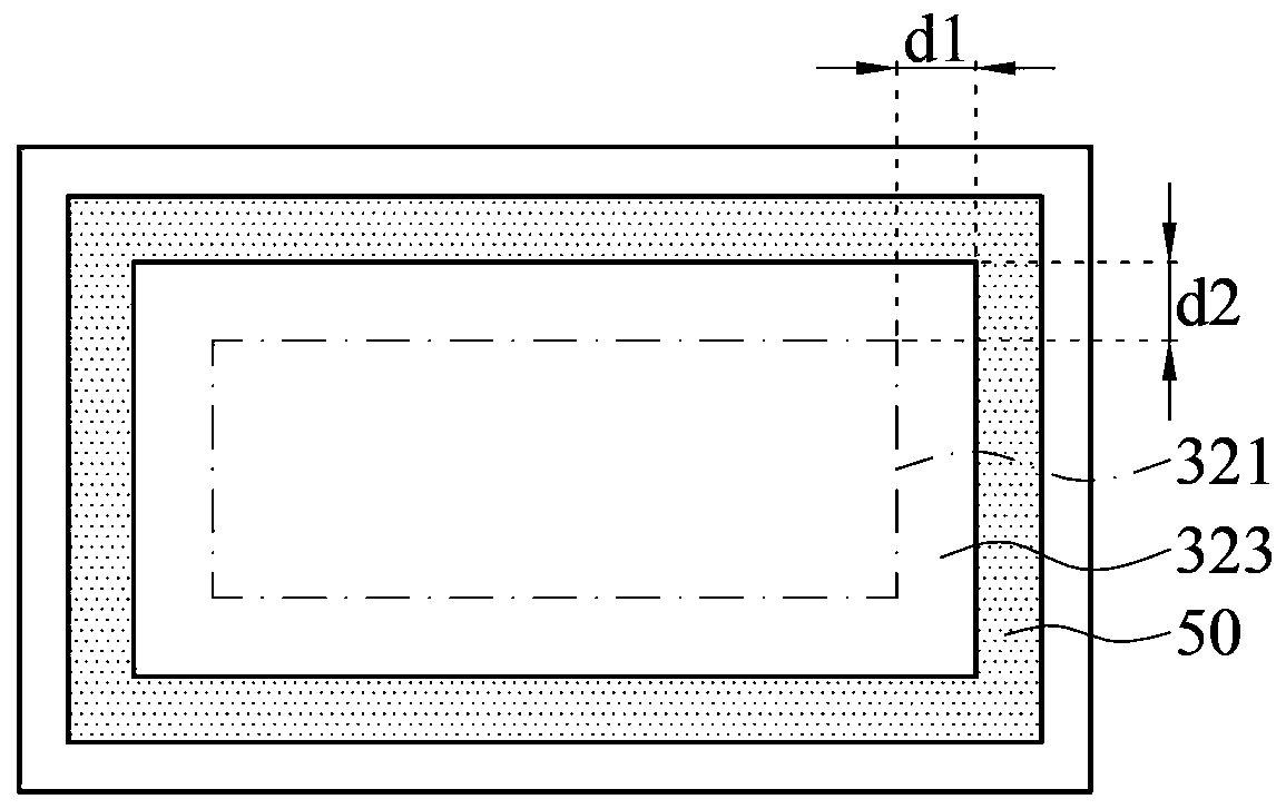
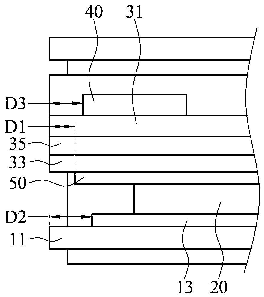
[0048] In the drawings, the widths of some elements, regions, etc. are exaggerated for clarity. Throughout the specification, the same reference numerals denote the same elements. It will be understood that when an element is referred to as being "on" or "connected to" another element, it can be directly on or connected to the other element or intervening elements may also be present. In contrast, when an element is referred to as being "directly on" or "directly connected to" another element, there are no intervening elements present.

[0049] It should be understood that although the terms "first", "second", "third", etc. may be used herein to describe various elements, components, regions, or sections, these elements, components, regions, and / or sections Should not be limited by these terms. These terms are only used to distinguish one element, component, region, or section from another element, component, region, layer or section. Thus, "a first element," "component," "...


PUM


Abstract

A touch device comprises an array substrate, a display medium layer, a filtering substrate, a touch electrode layer and a shielding electrode layer. The display dielectric layer is located on the array substrate. The filtering substrate is located on the display medium layer and corresponds to the array substrate, an active area and a peripheral area are defined by the filtering substrate, and theactive area is surrounded by the peripheral area. The touch electrode layer is located on the filter substrate. The shielding electrode layer is located between the light filtering substrate and thedisplay dielectric layer, and the vertical projection of the shielding electrode layer to the light filtering substrate is located in the peripheral area and surrounds the active area. Through the arrangement of the shielding electrode layer and the layout mode that the active area is surrounded by the vertical projection of the filtering substrate, the shielding effect is achieved, the noise problem of the touch device on the edge of the active area is greatly reduced, and the touch sensitivity and accuracy are improved.

Description

technical field [0001] The invention relates to the field of electronic motors, in particular to a touch device. Background technique [0002] A traditional touch panel has a touch layer, array electrodes and common electrodes for display functions. Since the layout of electrodes around the panel is different from that in the center of the panel, it is easy to cause uneven electric field. Therefore, it is easy to generate noise during signal transmission. [0003] These phenomena are especially obvious around the active area (display area) of the touch panel, where the noise is relatively large and interferes with the touch sensitivity. [0004] Especially when the stylus is used for operation, these noises will cause obvious sensitivity failure, which will cause inconvenience in touch operation. Contents of the invention [0005] In view of this, a touch device is provided herein. The touch device includes an array substrate, a display medium layer, a filter substrate,...

Claims


Application Information

Patent Timeline
Patent Type & Authority Applications(China)
IPC IPC(8): G06F3/041G06F3/0354
CPCG06F3/041G06F3/03545
Inventor 林韦霖邱孝豪
Owner AU OPTRONICS CORP
Why Eureka
Try Eureka