A voltage control device and system

A voltage control and controller technology, applied in the field of communication, can solve problems such as reducing transmission power, pin heating, abnormal system operation, etc., to meet power consumption requirements, increase power consumption, and ensure compatibility

Active Publication Date: 2020-10-02
深圳市联洲国际技术有限公司
View PDF8 Cites 0 Cited by
  • Summary
  • Abstract
  • Description
  • Claims
  • Application Information

AI Technical Summary

Problems solved by technology

However, this will cause the pins of the MINI PCIE interface to heat up seriously due to excessive current, and reduce the transmission power; at the same time, the total voltage drop on the transmission path will also increase with the increase of the current, resulting in finally reaching the MINI PCIE interface. The voltage of the card terminal equipment is much lower than its normal working voltage, which causes the system to work abnormally

Method used


Image

  • A voltage control device and system
  • A voltage control device and system
  • A voltage control device and system

Examples


Embodiment 1

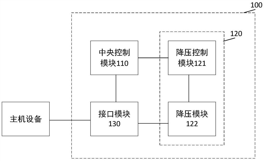
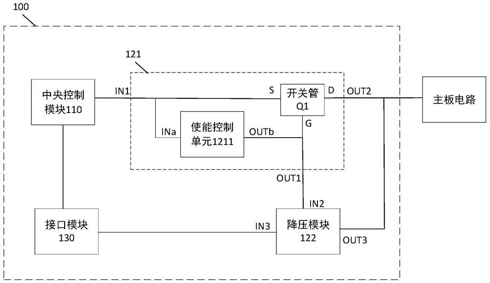
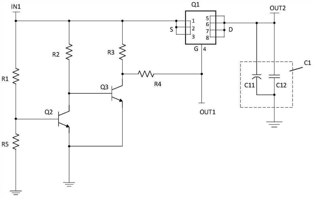
[0048] see figure 1 , is a schematic structural diagram of the first voltage control device 100 provided in Embodiment 1 of the present invention. The voltage control device 100 includes a central control module 110, a step-down controller 120 and an interface module 130; wherein the step-down controller 120 is connected to the central control module 110 and the interface module 130 respectively, and the central The control module 110 is connected with the interface module 130, and the interface module 130 is also used for connecting with a host device.

[0049] The central control module 110 is used to send a boost request to the host device, so that the host device can determine whether it has a boost function, and when it has a boost function, the output voltage is raised to a target voltage and output; The interface module 130 receives the target voltage.

[0050] When the host device has a boost function and the target voltage is greater than a preset standard voltage, ...

Embodiment 2

[0077] see Figure 5 , is a schematic structural diagram of the second voltage control device 200 provided in Embodiment 2 of the present invention. The voltage control device 200 includes a CPU module 210, a boost controller 220 and a socket module 230; wherein, the boost controller 220 is connected to the CPU module 210 and the socket module 230 respectively, and the CPU module 210 is connected to the socket module 230. The socket module 230 is connected, and the socket module 230 is also used to connect the interface device;

[0078] When establishing a connection with the interface device, the CPU module 210 determines whether a boost request sent by the interface device is received.

[0079] If so, the boost controller 220 boosts its output voltage to a target voltage according to the boost request, and the socket module 230 outputs the target voltage to the interface device, so that the interface device When it is determined that the target voltage is greater than a pr...

Embodiment 3

[0094] see Figure 7 , is a schematic structural diagram of a voltage control system 300 provided in Embodiment 3 of the present invention. The voltage control system 300 includes an interface device and a host device, the interface device is connected to the host device; wherein, the interface device includes the voltage control device 100 as described in Embodiment 1; the host device includes the implementation of The voltage control device 200 described in the second example. For the specific structural devices of the voltage control device 100 and the voltage control device 200 , refer to the first and second embodiments above, and details will not be repeated here.

[0095] see Figure 8 , is a schematic flowchart of the working process of the voltage control system 300 provided in the third embodiment of the present invention. When the MINI PCIE interface of the interface device is inserted into the MINI PCIE slot of the host device, the host device provides a standar...


PUM


Abstract

The invention discloses a voltage control device. The device comprises a central control module, a voltage reduction controller and an interface module. The central control module is used for sendinga boosting request to a host device, so that the host device determines whether the host device has a boosting function or not, and when the host device has the boosting function, the output voltage is boosted to a target voltage and output; the interface module receives the target voltage; and when the host device has the boosting function and the target voltage is greater than a preset standardvoltage, the voltage reduction controller reduces the target voltage to be equal to the standard voltage to serve as a working voltage. The invention further discloses another voltage control device and another voltage control system, and the total power consumption of the interface device can be improved by improving the output voltage of the host device, so that the power consumption requirementof the interface device is met, the voltage drop and the energy loss of a power supply path are effectively reduced, and the stability and the compatibility of the system are ensured.

Description

technical field [0001] The present invention relates to the field of communication technology, in particular to a voltage control device and system. Background technique [0002] The MINI PCIE (Mini PCI Express) interface is a general-purpose circuit interface consisting of a plug-in card and a connector. For a standard MINI PCIE card, affected by its own power supply specifications, the maximum peak power consumption it can obtain is relatively low. With the rapid development of communication networks, the specifications of wireless devices have developed explosively. For terminal devices using MINI PCIE cards, the demand for single-board power consumption is high, far exceeding the maximum peak power that standard MINI PCIE cards can provide. At this time, the power consumption of the standard MINI PCIE interface can no longer meet the demand. [0003] In the prior art, power consumption is improved by increasing the power supply current of the MINI PCIE interface. Howe...

Claims


Application Information

Patent Timeline
Patent Type & Authority Patents(China)
IPC IPC(8): H02M3/158
CPCH02M3/1582
Inventor 钟宝万
Owner 深圳市联洲国际技术有限公司
Why Eureka
Try Eureka