
Flexible circuit board and manufacturing method of said flexible circuit board

A technology of flexible circuit boards and manufacturing methods, which is applied in the fields of printed circuit manufacturing, printed circuits, and removal of conductive materials by chemical/electrolytic methods, which can solve the problems of inability to accurately align electronic chips, and achieve better flexibility and satisfy The effect of counterpoint requirements

Active Publication Date: 2021-11-02
AVARY HLDG (SHENZHEN) CO LTD +1
View PDF7 Cites 0 Cited by
  • Summary
  • Abstract
  • Description
  • Claims
  • Application Information

AI Technical Summary

Problems solved by technology

However, after the inner circuit is fabricated, due to a series of follow-up processes, the size of the multi-layer circuit board will change greatly, so that the final electronic chip cannot be accurately aligned.

Method used


Image

  • Flexible circuit board and manufacturing method of said flexible circuit board
  • Flexible circuit board and manufacturing method of said flexible circuit board
  • Flexible circuit board and manufacturing method of said flexible circuit board

Examples


Embodiment Construction

[0023] In order to further explain the technical means and effects adopted by the present invention to achieve the intended purpose of the invention, the specific implementation, structure, characteristics and effects of the method for manufacturing a flexible circuit board provided by the present invention will be described below in conjunction with the accompanying drawings and preferred embodiments. A detailed description is made as follows.

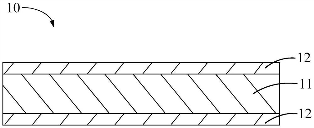
[0024] see Figure 1-11 , the present invention provides a method for manufacturing the flexible circuit board 100 . According to different requirements, the order of steps in the method for manufacturing the flexible circuit board 100 can be changed, and some steps can be omitted or combined. The manufacturing method of the flexible circuit board 100 includes the following steps:

[0025] Step one, see figure 1 , providing a double-sided copper clad substrate 10 . The double-sided copper clad substrate 10 includes a flexible base...


PUM


Abstract

A method for manufacturing a flexible circuit board, comprising: providing a double-sided copper-clad substrate; etching the first copper layer to obtain two first circuit layers; covering each first circuit layer with a first adhesive layer, a first insulating Layer and the second copper layer, etch the second copper layer to obtain two second circuit layers; cover the second adhesive layer and the second insulating layer on each second circuit layer; in each second insulating layer A third copper layer is formed on the surface, and the third copper layer is etched to obtain two third circuit layers; a third glue layer and a protective layer are covered on each third circuit layer; A first groove and a second groove are provided in the third adhesive layer, and a groove is opened at a position corresponding to the second groove from one of the protective layers to the second adhesive layer on the other side of the base layer, thereby The second insulating layer on one side of the second groove and the corresponding third wiring layer form a single-panel area at a portion corresponding to the groove.

Description

technical field [0001] The invention relates to a printed circuit board technology, in particular to a flexible circuit board and a manufacturing method of the flexible circuit board. Background technique [0002] Nowadays, more and more electronic products such as smartphones and tablet computers use active matrix organic light emitting diode (AMOLED) screens. For the high integration requirements of this type of screen, the high-density wiring of the flexible circuit board used to drive the screen will face many challenges. [0003] A conventional flexible circuit board includes inner circuits and outer circuits, and electronic chips for driving the screen are mounted on the inner circuits. In order to meet the alignment requirements of the center pitch of the electronic chip pins, the line width and line pitch of the inner layer circuits usually need to be less than 10 μm / 10 μm. However, after the inner circuit is fabricated, the size of the multi-layer circuit board wi...

Claims


Application Information

Patent Timeline
Patent Type & Authority Patents(China)
IPC IPC(8): H05K3/10H05K3/06H05K1/02
CPCH05K1/028H05K3/06H05K3/108
Inventor 胡先钦沈芾云何明展
Owner AVARY HLDG (SHENZHEN) CO LTD
Learn More