Semiconductor laser element
A technology of laser components and semiconductors, applied in the direction of semiconductor lasers, laser components, lasers, etc., can solve problems such as no solutions, and achieve the effect of increasing the working temperature
- Summary
- Abstract
- Description
- Claims
- Application Information
AI Technical Summary
Problems solved by technology
Method used
Image

Examples
Embodiment 1
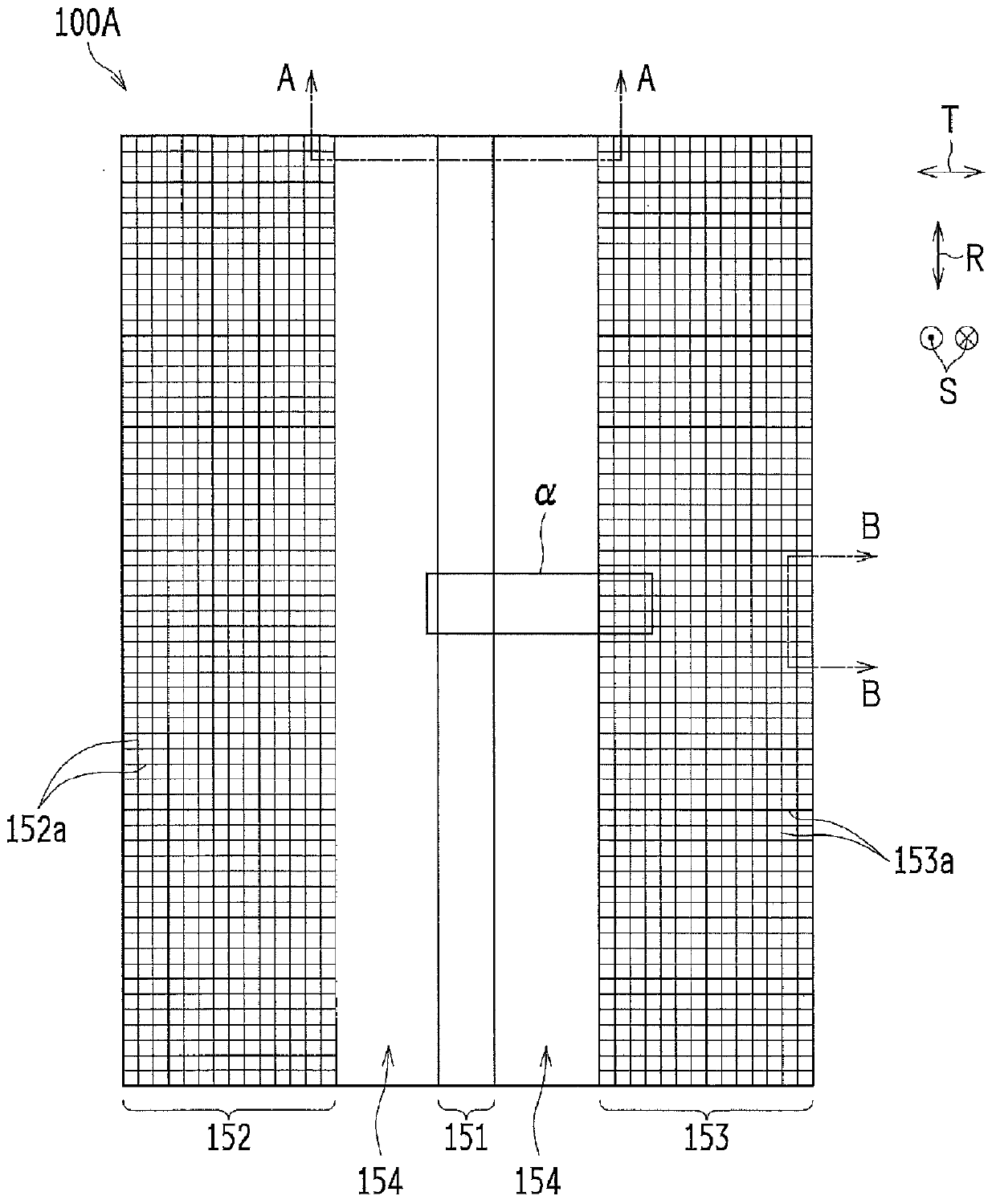
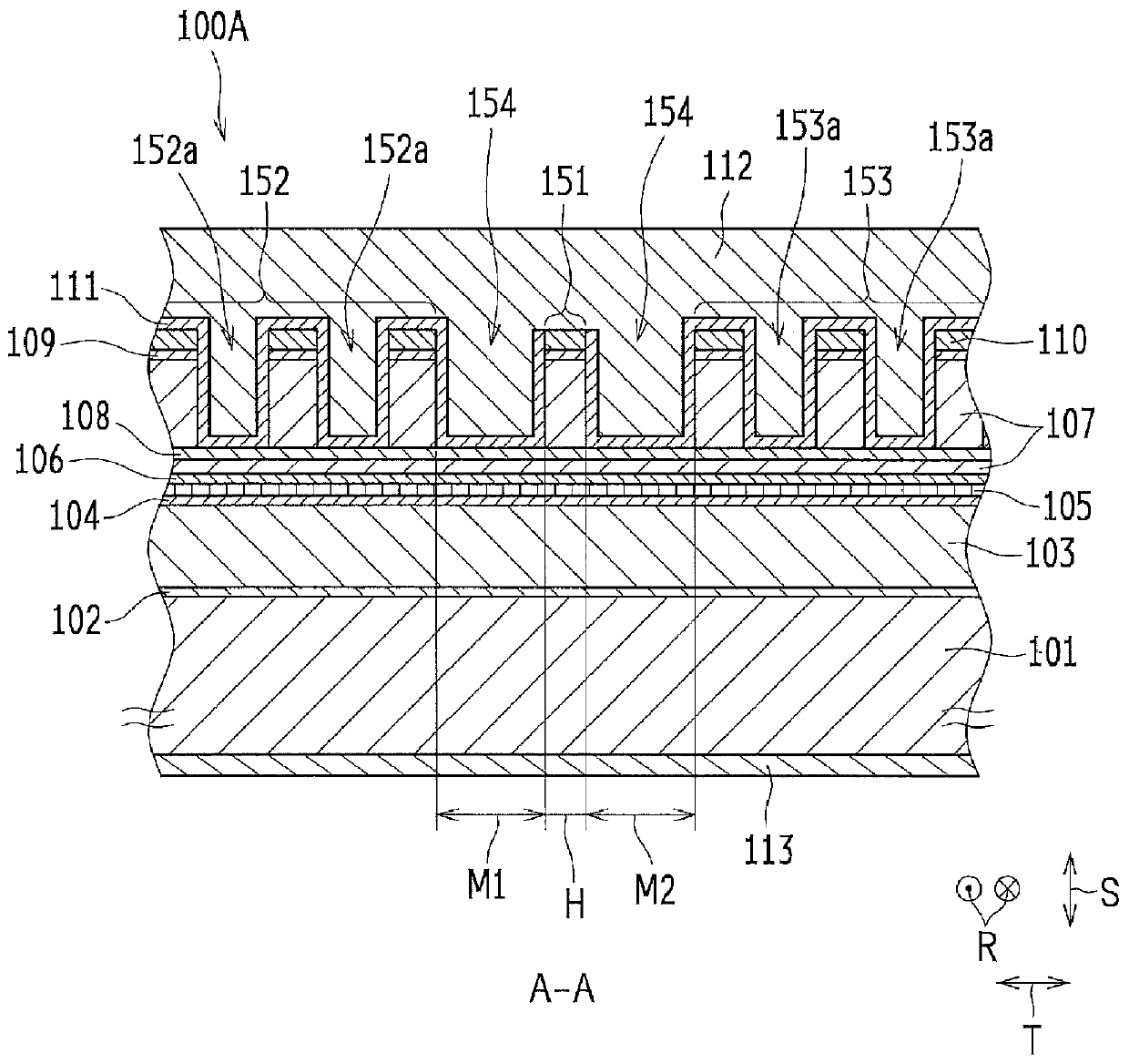
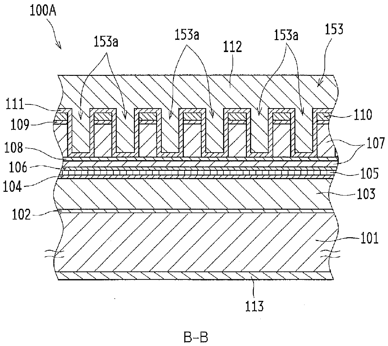
[0040] figure 1 It is a plan view schematically showing the semiconductor laser element 100A of the first embodiment. In addition, in figure 1 In, SiO is omitted 2 Illustration of membrane 111 and TiAu / Au plated electrode 112. figure 2 is along figure 1 A schematic cross-sectional view of the semiconductor laser element 100A of the first embodiment taken along the line A-A shown. image 3 is along figure 1 A schematic cross-sectional view of the semiconductor laser element 100A of the first embodiment taken along the line B-B shown.
[0041] Figure 4 It shows the semiconductor laser element 100A of the first embodiment viewed obliquely from above. figure 1 A perspective view of the region α shown.
[0042] Such as figure 1 and figure 2 As shown, on the basis of n-type GaAs substrate 101, semiconductor laser element 100A also includes: n-type GaInP buffer layer 102 formed on n-type GaAs substrate 101 by metal-organic vapor phase epitaxy, n-type AlGaInP first ...
Embodiment 2
[0057] Figure 5 It is a schematic plan view schematically showing an example of the semiconductor laser element 100B of the second embodiment.
[0058] The epitaxial structure of the semiconductor laser element 100B of the second embodiment is substantially the same as the epitaxial structure of the semiconductor laser element 100A of the first embodiment. The semiconductor laser element 100B of the second embodiment is manufactured by the same manufacturing process as that of the first embodiment.
[0059] In the second embodiment, in the semiconductor laser element 100B, the resonator length is 1500 μm, the chip width is 110 μm, and the width H of the ridge 151 is 1.7 μm. In addition, in the semiconductor laser element 100B, the terrace portions 152 , 153 are separately provided in the resonator direction R in a plurality (three in this example) of separation stages 1521 to 1523 and 1531 to 1533 . Separation stages 1521 to 1523 and 1531 to 1533 are formed at a predetermin...
Embodiment 3
[0063] Figure 6 It is a schematic plan view schematically showing an example of the semiconductor laser element 100C of the third embodiment.
[0064] The epitaxial structure of the semiconductor laser element 100C of the third embodiment is substantially the same as the epitaxial structure of the semiconductor laser element 100A of the first embodiment. The semiconductor laser element 100C of the third embodiment is manufactured by the same manufacturing process as that of the first embodiment.
[0065] In the third embodiment, in the semiconductor laser element 100C, the resonator length is 800 μm, the chip width is 110 μm, and the width of the ridge 151 is 2.0 μm. In the semiconductor laser element 100C, the terrace portions 152 , 153 are provided at four corners of corner portions where one side along the resonator direction R intersects one side along the width direction T. The terrace portions 152, 153 are formed in a triangular shape such that the apex corners are al...
PUM
 Abstract
Description
Claims
Application Information
 - R&D
- Intellectual Property
- Life Sciences
- Materials
- Tech Scout
- Unparalleled Data Quality
- Higher Quality Content
- 60% Fewer Hallucinations
Browse by: Latest US Patents, China's latest patents, Technical Efficacy Thesaurus, Application Domain, Technology Topic, Popular Technical Reports.
© 2025 PatSnap. All rights reserved.Legal|Privacy policy|Modern Slavery Act Transparency Statement|Sitemap|About US| Contact US: help@patsnap.com