Integrated packaging LED display panel based on chip stacking

An integrated packaging and chip stacking technology, applied in the field of integrated packaging LED display panels, can solve the problems of easy de-soldering of welding pins, high pollution, and many out-of-control points of pixels, so as to solve the problem of out-of-pixel failure, reduce pollution emissions, pixel The effect of small spacing

Pending Publication Date: 2019-12-20
深圳韦侨顺光电有限公司
View PDF0 Cites 5 Cited by
  • Summary
  • Abstract
  • Description
  • Claims
  • Application Information

AI Technical Summary

Problems solved by technology

Because this technology only solves the problem of exposed bracket pins of the driver IC package module originally placed on the back of the lamp bead on the LED driver integrated PCB board, it does not solve the problem of exposed bracket pins of the dual-function chip SMD package device, it is not completely useless The standoff leadless packaging technology cannot fundamentally solve the problem of many out-of-control pixels caused by the standoff pins of SMD packaged devices. Waste of cutting-edge equipment resources and human resources
[0005] 2. Another defect of packaged devices with bracket pins is that the packaged devices have low anti-knock ability, and the soldered pins are easy to desolder when performing flexible bending applications
[0006] 3. The driver IC bare chip is implanted into the dual-function chip SMD package device. Due to the large size of the chip itself and the arrangement on the same level as the LED bare chip chip, the appearance and volume of the dual-function chip SMD package device are relatively large. , the pixel pitch of the display panel cannot exceed 3mm or less
[0007] 4. Due to the large size of the driver IC bare chip and many welding lines, it increases the difficulty of the dual-function chip SMD packaging process
[0008] 5. Due to the large size of the driver IC bare chip, it will affect the normal light output of the LED chip at certain angles and affect the optical display effect of the packaged device
[0010] 7. The management and control of the production process is complicated, and there are too many factors affecting the reliability of display panel products, which is not conducive to the development of intelligent production
[0011] 8. The display panel technology of two boards results in twice the waste of printed circuit board or display panel substrates
The printed circuit board industry is a high-pollution, high-carbon-emission industry, and the environmental assessment value of this display panel technology is low
[0012] 9. Low design integration, low process integration and low industrial integration

Method used


Image

  • Integrated packaging LED display panel based on chip stacking
  • Integrated packaging LED display panel based on chip stacking
  • Integrated packaging LED display panel based on chip stacking

Examples


Embodiment Construction

[0030] Below in conjunction with specific embodiment and accompanying drawing, the present invention is further elaborated and illustrated:

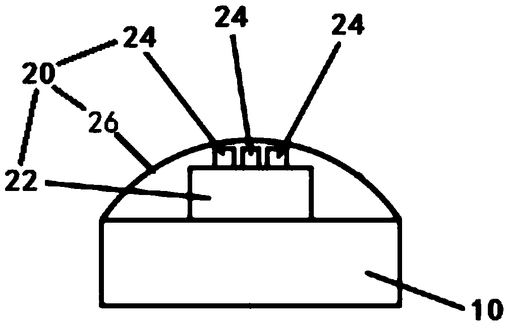
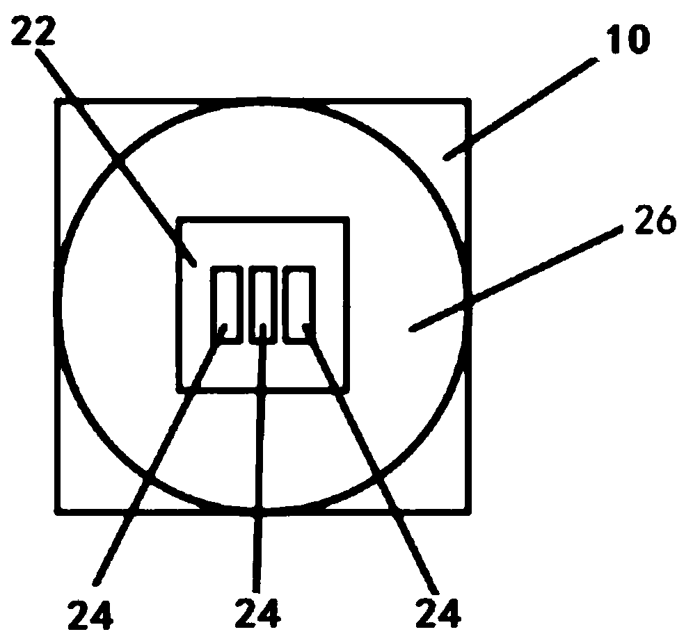
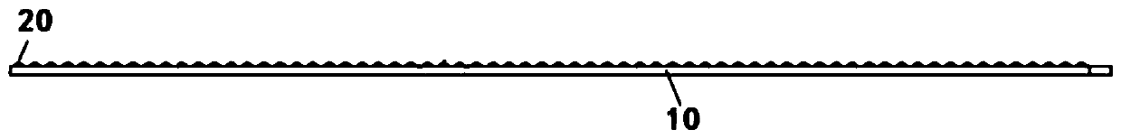
[0031] Please refer to figure 1 , figure 2 with image 3 , the integrated packaged LED display panel based on chip stacking includes an integrated packaged circuit board 10, and the integrated packaged circuit board is provided with at least two integrated packaged lamp beads 20 without support pins. The integrated packaged lamp bead 20 without support pins includes a driver IC bare chip 22, an LED bare chip 24 and an encapsulant 26, and the LED bare chip 24 is stacked on the upper surface of the driver IC bare chip 22 and connected to the driver IC bare chip 22. The bare IC chip 22 is electrically connected, and after the bare driver IC chip 22 is electrically connected to the integrated packaging circuit board 10 , the packaging compound 26 encapsulates the bare driver IC chip 22 and the bare LED chip 24 .

[0032] The LED die chip...


PUM


Abstract

The invention discloses an integrated packaging LED display panel based on chip stacking. The display panel comprises an integrated packaging circuit board, and the integrated packaging circuit boardis provided with at least two integrated packaging lamp beads. The integrated packaging lamp bead without the support pin comprises a driving IC bare crystal chip, an LED bare crystal chip and a packaging colloid. The LED bare crystal chip is stacked on the upper surface of the driving IC bare crystal chip and is electrically connected with the driving IC bare crystal chip; after the driving IC bare crystal chip is electrically connected with the integrated packaging circuit board, the packaging colloid packages the driving IC bare crystal chip and the LED bare crystal chip. According to the integrated packaging LED display panel based on chip stacking, the multifunctional high integration is achieved, support-pin-free lamp driving is integrated with pixel integrated packaging, and the effects of high lightness, thinness, structure-free mounting, high product quality, high display pixel density and high display effect are achieved.

Description

technical field [0001] The invention relates to the technical field of LEDs, in particular to an integrated packaging LED display panel based on chip stacking. Background technique [0002] The existing LED display panel of similar technology is realized by SMD packaging devices, and the SMD packaging device colloid is arranged with a driver IC bare chip and an LED bare chip, and the spatial position relationship between the driver IC bare chip and the LED bare chip It is a flat and horizontal arrangement. It is a single-pixel independent packaged device with bracket pins. After the dual-function chip SMD packaged device is packaged, it is mounted on a matrix or non-matrix multi-group lamp by SMT welding process. The LED display panel of this packaged device is manufactured on the circuit board of the bit pad, which is a two-board independent packaged device with bracket pins packaged and SMT welding process LED display panel manufacturing technology. [0003] This LED disp...

Claims


Application Information

Patent Timeline
Patent Type & Authority Applications(China)
IPC IPC(8): H01L25/16G09F9/33
CPCG09F9/33H01L25/167
Inventor 梁青胡志军
Owner 深圳韦侨顺光电有限公司
Why Eureka
Try Eureka