Data processing method and device

A data processing and processor technology, which is applied in electrical digital data processing, input/output process of data processing, instruments, etc., and can solve the problems of high cost and large usage of RAM

Active Publication Date: 2019-12-24
BOE TECH GRP CO LTD
View PDF7 Cites 1 Cited by
  • Summary
  • Abstract
  • Description
  • Claims
  • Application Information

AI Technical Summary

Problems solved by technology

[0004] The object of the present invention is to provide a kind of data processing method and device, when storing pixel data in the prior art, the usage amount of the block random access memory is larger, causes the problem that the cost of FPGA is high

Method used


Image

  • Data processing method and device
  • Data processing method and device
  • Data processing method and device

Examples


Embodiment Construction

[0034] In order to make the technical problems, technical solutions and advantages to be solved by the present invention clearer, the following will describe in detail with reference to the drawings and specific embodiments.

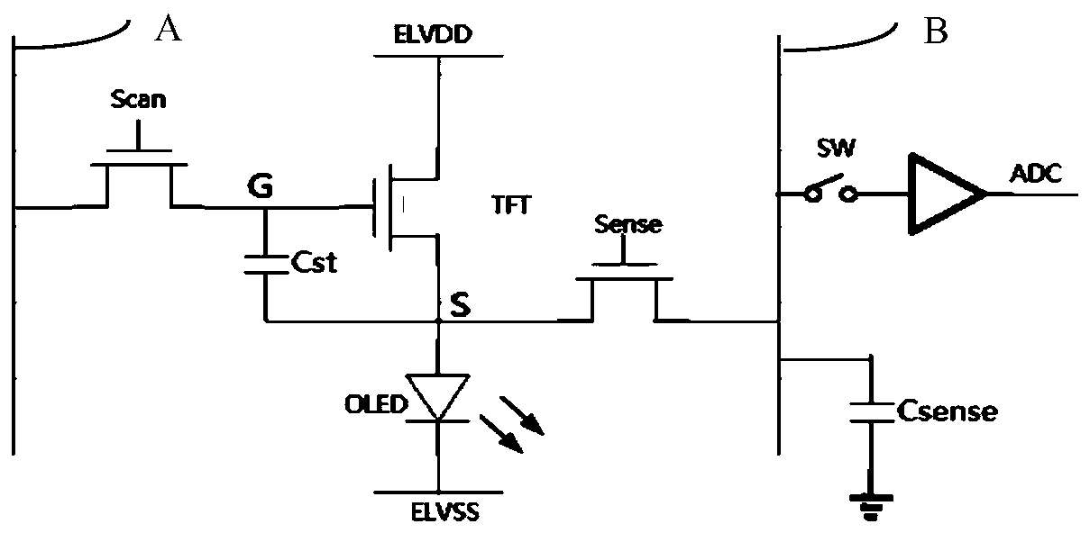
[0035] figure 1 It is the large-size OLED pixel compensation circuit at the present stage. The label A in the figure shows the data line (Data Line), and the label B shows the sensing line (Sense Line). The basic principle of compensation is:

[0036] Initialization stage: Turn on the Scan and Sense switches, and the Data Line is given a known voltage V data , Sense Line given reset voltage V ref , and have V data >V ref ;

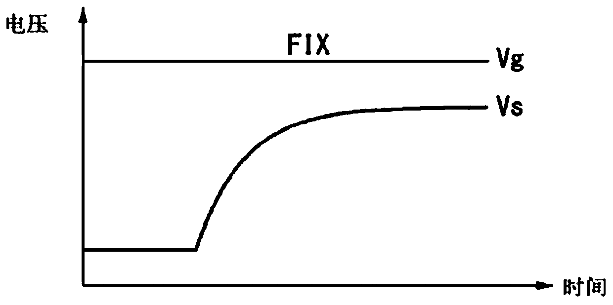
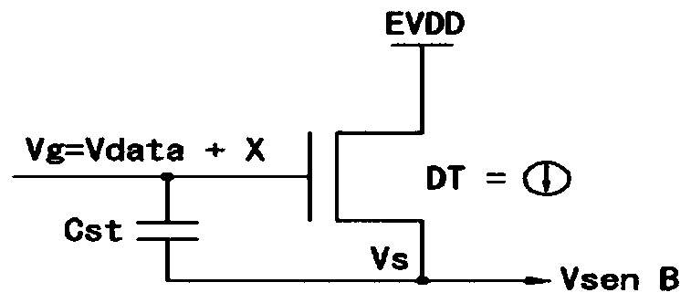
[0037] Charging stage: Turn on the Scan and Sense switches, because V data >V ref , the Driving TFT (TFT in the figure) is turned on to generate current through the Sense switch to the capacitance C of the Sense Line sense Charging, when the voltage of Sense Line (point S) is charged to V data -V th , the Driving TFT is cut ...


PUM


Abstract

The embodiment of the invention provides a data processing method and a device, and the method comprises the steps: obtaining the data information of pixels in a display device, and the data information comprises the compensation data of the pixels and the position of the pixels; according to a preset mapping relationship, determining a storage position of compensation data of the pixels in a block random access memory, wherein the block random access memory comprises a plurality of groups of data units which are stored in sequence, the sequences in which the data units with adjacent storage positions are taken out are adjacent, the data units comprise a plurality of compensation data which are taken out in the same clock period, and the plurality of compensation data are stored in the block random access memory in sequence; and storing the compensation data in a storage space corresponding to the storage position. Therefore, the compensation data can be preferentially stored in one block random access memory, the storage capacity of the block random access memory is fully utilized, and the use number of the block random access memory is reduced, so that the cost of the FPGA is reduced.

Description

technical field [0001] The present invention relates to the field of display technology, in particular to a data processing method and device. Background technique [0002] Large-sized organic light-emitting semiconductor (Organic Light-Emitting Diode referred to as OLED) needs to be compensated during the display process. During the compensation process, the driver IC will send the sensing data back to the timing controller (TimerController, referred to as TCON), TCON The sensing data is obtained to compensate the OLED threshold voltage and mobility to the OLED. In the process of driving and calculating the compensated OLED threshold voltage and mobility according to the algorithm, a programmable logic gate array (Field Programmable Gate Array, FPGA for short) is used to realize. [0003] When the algorithm is implemented, a large number of FPGA internal storage resources are needed, that is, block random access memory (Block RAM, Random Access Memory, referred to as RAM)....

Claims


Application Information

Patent Timeline
Patent Type & Authority Applications(China)
IPC IPC(8): G09G3/3208G06F3/147
CPCG06F3/147G09G3/3208
Inventor 陈燚
Owner BOE TECH GRP CO LTD
Why Eureka
Try Eureka