Clearing device, photoetching apparatus and photoetching method

A technology of cleaning device and lithography equipment, applied in microlithography exposure equipment, optomechanical equipment, photolithography process exposure device, etc., can solve the problem of grating panel being difficult to clean, and reduce the probability of wiping or replacing grating panel, The effect of reducing secondary pollution, improving convenience and reliability

Active Publication Date: 2020-01-07
SHANGHAI MICRO ELECTRONICS EQUIP (GRP) CO LTD
View PDF4 Cites 0 Cited by
  • Summary
  • Abstract
  • Description
  • Claims
  • Application Information

AI Technical Summary

Problems solved by technology

[0005] The purpose of the present invention is to provide a clearing device, photolithography equipment and photolithography method to solve the problem that the grating panel is not easy to clean in the prior art

Method used


Image

  • Clearing device, photoetching apparatus and photoetching method
  • Clearing device, photoetching apparatus and photoetching method
  • Clearing device, photoetching apparatus and photoetching method

Examples


Embodiment Construction

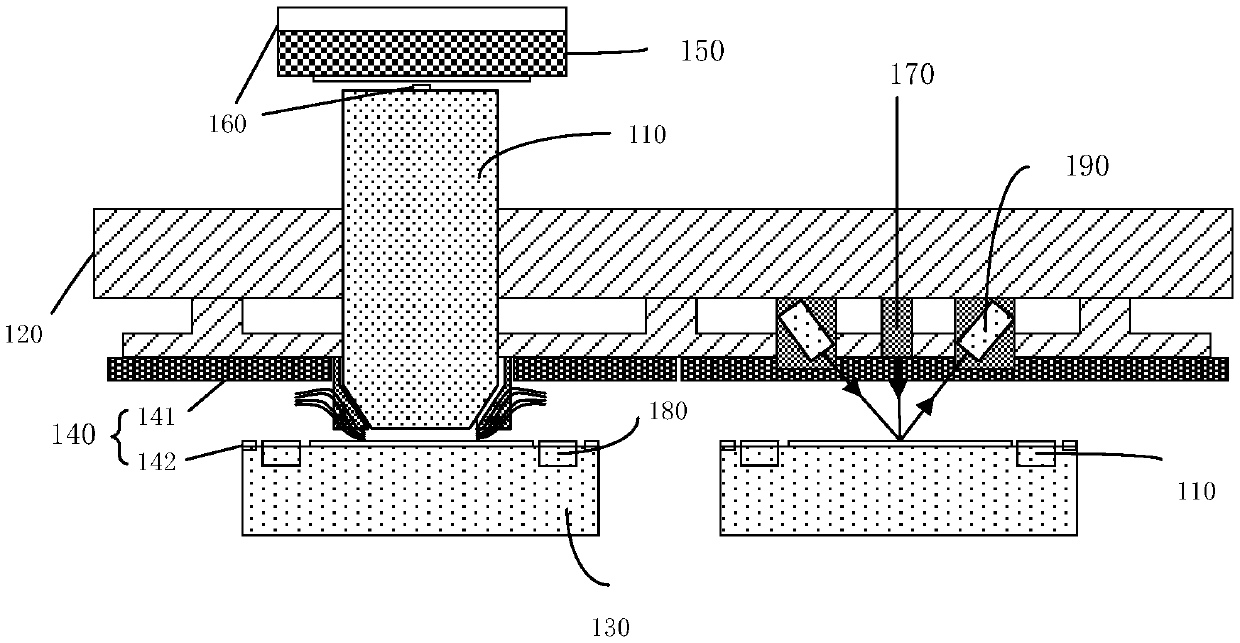
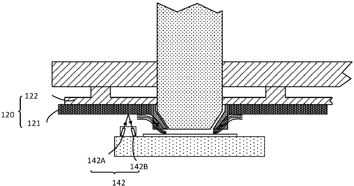
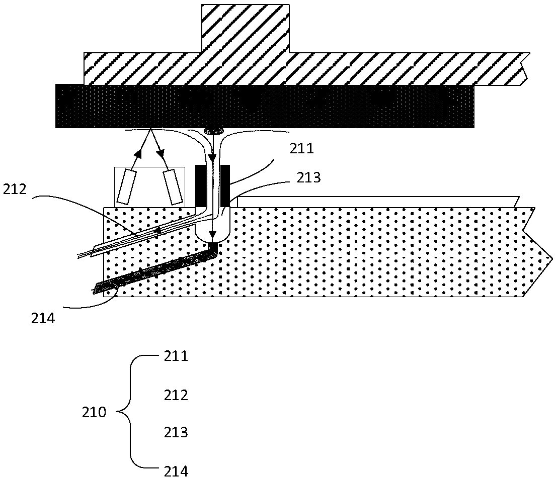
[0043] The specific implementation manner of the present invention will be described in more detail below with reference to schematic diagrams. Advantages and features of the present invention will be apparent from the following description and claims. It should be noted that all the drawings are in a very simplified form and use imprecise scales, and are only used to facilitate and clearly assist the purpose of illustrating the embodiments of the present invention.

[0044] refer to Figure 3 to Figure 5, the present invention provides a cleaning device 210, the cleaning device 210 includes: an adsorption unit 211 and a negative pressure channel 212;

[0045] The adsorption unit 211 is arranged on the surface of a workpiece table facing the bearing surface of the object to be removed, the negative pressure channel 212 is located inside the workpiece table, and the negative pressure channel 212 communicates with the adsorption unit 211 and communicates with the adsorption uni...


PUM

PropertyMeasurementUnit
sizeaaaaaaaaaa

Abstract

The invention provides a clearing device, a photoetching apparatus and a photoetching method. The clearing device comprises an adsorption unit and a negative pressure channel; the adsorption unit is located on the surface of a workpiece table; the negative pressure channel is located in the workpiece table; the negative pressure channel is communicated with the adsorption unit and provides negative pressure for the adsorption unit; and if a grating panel contains immersion liquid, the immersion liquid can be absorbed by means of negative pressure, so that the grating panel can be cleaned, andtherefore, the probability of wiping or replacing the grating panel is reduced, secondary pollution to the grating panel can be reduced, and the convenience and reliability of cleaning the grating panel are improved.

Description

technical field [0001] The invention relates to the technical field of semiconductor manufacturing equipment, in particular to a cleaning device, photolithography equipment and a photolithography method. Background technique [0002] a kind of like figure 1 The photolithography equipment shown is mainly composed of the following key subsystems: objective lens group 110, frame 120 supporting all movement and measurement mechanisms, workpiece stage 130 carrying silicon wafers, workpiece stage positioning measurement sensor 140, and Mask stage 150 , mask stage positioning measurement sensor 160 , silicon wafer horizontal position measurement sensor 170 , mask position measurement sensor 180 , silicon wafer vertical position measurement sensor 190 , etc. Among these subsystems, the core is the positioning of the workpiece table (that is, the positioning subsystem), and high-precision sensors are usually used as positioning sensors. [0003] In order to improve productivity and...

Claims


Application Information

Patent Timeline
Patent Type & Authority Applications(China)
IPC IPC(8): G03F7/20
CPCG03F7/2041G03F7/70341G03F7/7085G03F7/70925G03F7/20
Inventor 吴丽丽
Owner SHANGHAI MICRO ELECTRONICS EQUIP (GRP) CO LTD
Why Eureka
Try Eureka