Fingerprint sensor package module made and process for making fingerprint sensor package module

A technology for encapsulating modules and fingerprints, which is used in the acquisition/organization of fingerprints/palmprints, character and pattern recognition, instruments, etc., and can solve the problems of the sensitivity of fingerprint sensing chips and the impact of process yield.

A technology for encapsulating modules and fingerprints, which is used in the acquisition/organization of fingerprints/palmprints, character and pattern recognition, instruments, etc., and can solve the problems of the sensitivity of fingerprint sensing chips and the impact of process yield.

CN110659554APending Publication Date: 2020-01-07TONG HSING ELECTRONICS IND LTD

Image

  • Fingerprint sensor package module made and process for making fingerprint sensor package module
  • Fingerprint sensor package module made and process for making fingerprint sensor package module
  • Fingerprint sensor package module made and process for making fingerprint sensor package module

Examples


no. 1 example

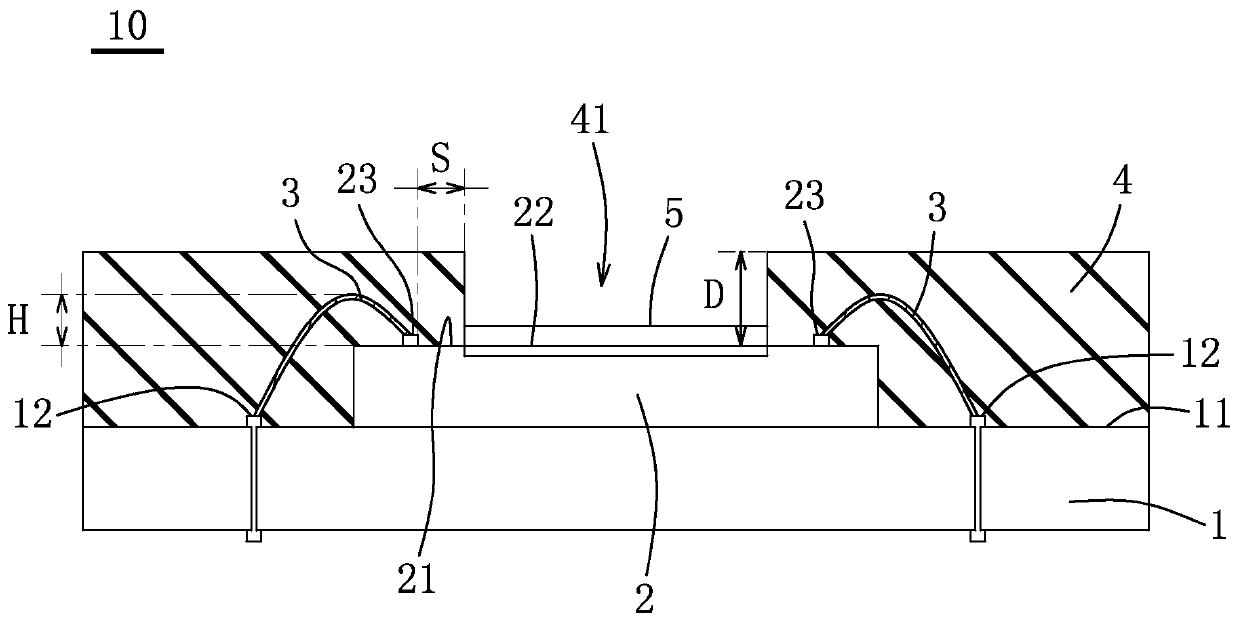
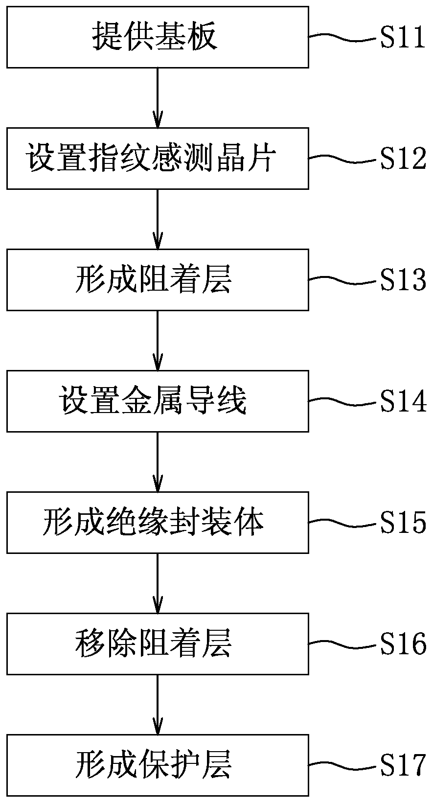
[0034] refer to figure 1 and figure 2 , is a first embodiment of the fingerprint sensing package module 10 and its manufacturing method of the present invention, the fingerprint sensing package module 10 includes a substrate 1, a fingerprint sensing chip 2, a plurality of metal wires 3, an insulating package Body 4, and a light-transmitting protective layer 5.

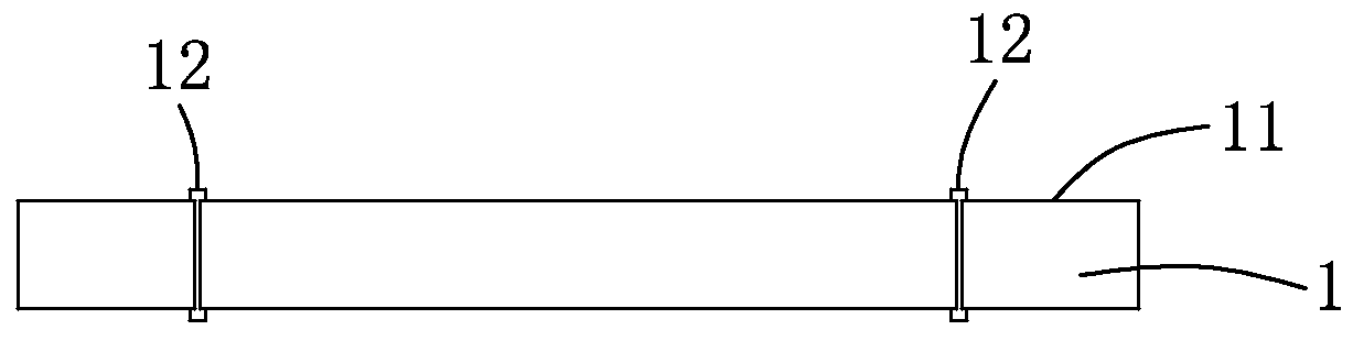
[0035] The substrate 1 is, for example, various types of circuit boards such as ceramic circuit boards, and includes a mounting surface 11 and a plurality of circuit contacts 12 disposed on the mounting surface 11 .

[0036] The fingerprint sensing chip 2 is arranged on the installation surface 11 of the substrate 1, and has a first surface 21 facing away from the installation surface 11, a chip located on the first surface 21 and suitable for fingerprint sensing. The sensing area 22, and a plurality of electrical contacts 23 arranged on the first surface 21 and adjacent to the periphery of the sensing area 22, the ...


PUM


Abstract

The invention discloses a fingerprint sensor package module made and a process for making the fingerprint sensor package module. The fingerprint sensor package module includes a substrate, a fingerprint sensing chip, a plurality of metal wires, and an insulating package. The substrate comprises a mounting surface and a plurality of circuit contacts arranged on the mounting surface. Wherein the fingerprint sensing chip is arranged on the mounting surface of the substrate, the fingerprint sensing chip is provided with a first surface back to the mounting surface, a sensing area located on the first surface and a plurality of electrical contacts arranged on the first surface and adjacent to the periphery of the sensing area, and the distance between the electrical contacts and the sensing area is smaller than 300 microns. The metal wire is bridged between the circuit contact and the electrical contact. The insulating package covers the mounting surface of the substrate, the fingerprint sensing chip and the metal wire, and an open groove for exposing the sensing area is formed in the insulating package. Therefore, the size of the fingerprint sensing chip is not too large, and the sizeof the f fingerprint sensor package module is reduced.

Description

technical field [0001] The invention relates to a fingerprint sensing packaging module, in particular to a fingerprint sensing packaging module and a manufacturing method thereof. Background technique [0002] Generally, after the important components are installed in the fingerprint sensing packaging module, the protective structure is usually made by sealing the glue. However, during the sealing process, the sealing material is easy to contaminate the sensing area of ​​the fingerprint sensing chip due to the overflow problem. The situation will affect the sensitivity of the fingerprint sensing chip and affect the process yield. [0003] In addition, because the fingerprint sensing package module is often used in various electronic devices such as mobile phones and laptops, and because the space for installing various modules in general electronic devices is very limited, reducing the volume of the fingerprint sensing package module is the design priority. An important sub...

Claims


Application Information

Patent Timeline
07 Jan 2020
Publication
CN110659554A
IPC
G06K9/00; G06V10/147
CPC
G06V40/12; H01L27/14678; H01L27/14618; H01L2224/48091; H01L2224/16225; H01L2224/8592; H01L2224/48227; H01L2924/1815
Inventors
张嘉帅