Guided inspection of a semiconductor wafer based on systematic defects

A semiconductor, defect technology, used in the field of guided inspection

Active Publication Date: 2020-01-07
APPL MATERIALS ISRAEL LTD
View PDF6 Cites 2 Cited by
  • Summary
  • Abstract
  • Description
  • Claims
  • Application Information

AI Technical Summary

Problems solved by technology

This fabrication process may require forming semiconductor device features with high prec

Method used


Image

  • Guided inspection of a semiconductor wafer based on systematic defects
  • Guided inspection of a semiconductor wafer based on systematic defects
  • Guided inspection of a semiconductor wafer based on systematic defects

Examples


Embodiment Construction

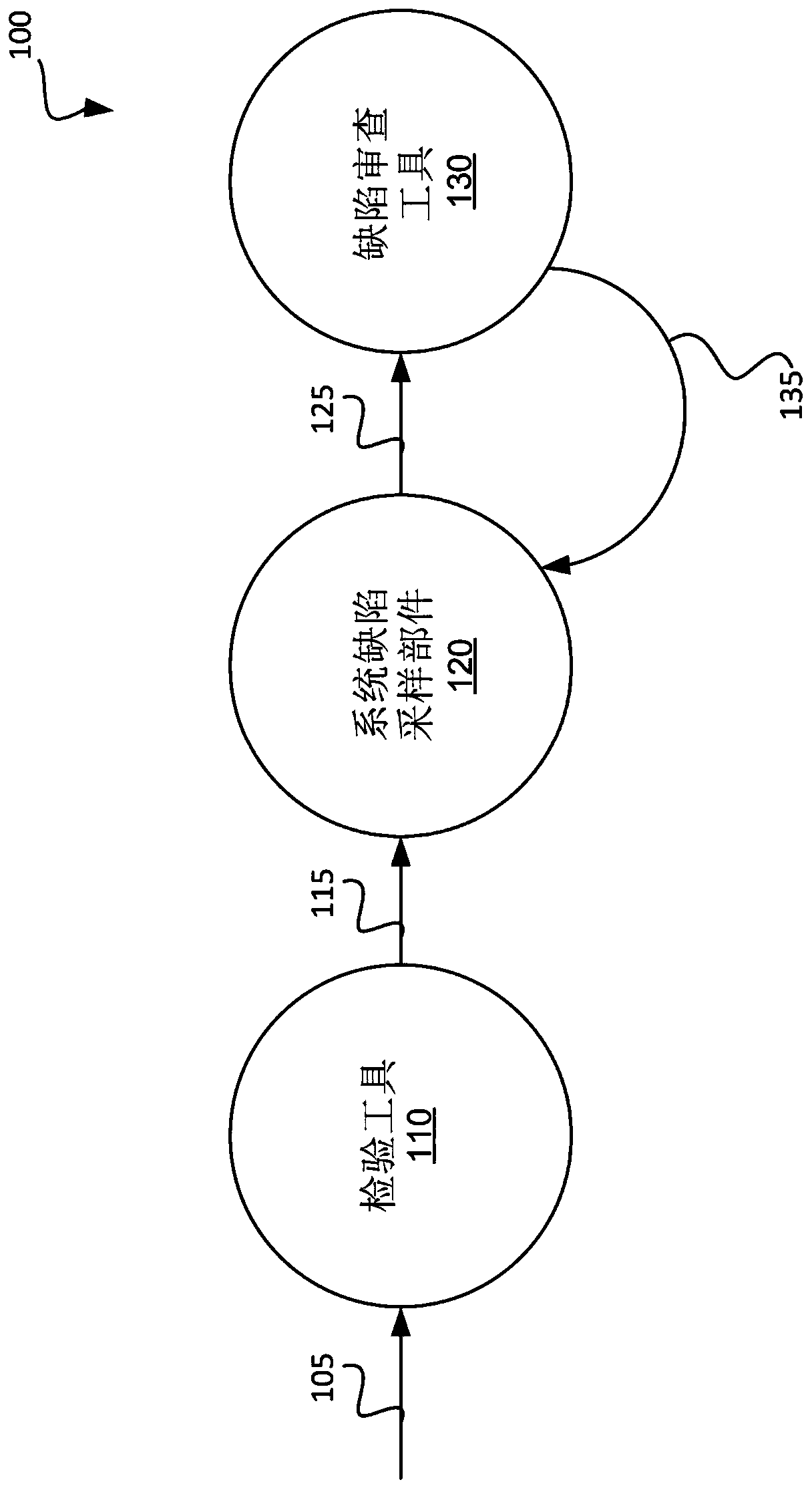
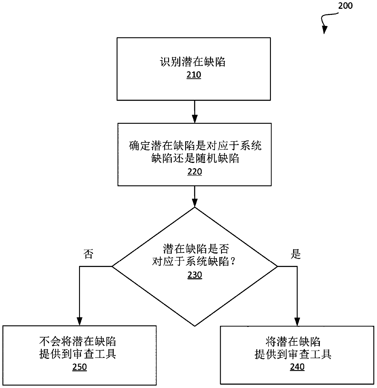
[0020] Aspects of the present disclosure relate to systematic defect-based guided inspection of semiconductor wafers. In general, semiconductor wafer inspection systems may be used to perform inspection of semiconductor wafers. For example, semiconductor wafer inspection systems may be used to identify defects at semiconductor wafers.

[0021] A semiconductor wafer inspection system may include optical tools and defect review tools. For example, optical tools may be used to identify potential or candidate defects at semiconductor wafers after or during the manufacturing process. Subsequently, a defect review tool may be used to examine, classify, or determine whether a candidate defect is an actual defect or not (eg, a "false alarm"). Where the design of the semiconductor wafer or other such technology (eg, fabrication process, material usage, or design features) is new, the fabrication process of the semiconductor wafer may be unstable and result in lower yields of semicond...


PUM


Abstract

A candidate defect may be identified at a semiconductor wafer. A determination may be made as to whether the candidate defect at the semiconductor wafer corresponds to a systematic defect or a randomdefect. In response to determining that the candidate defect at the semiconductor wafer corresponds to a systematic detect, the candidate defect at the semiconductor wafer may be provided to a defectreview tool for review by the defect review tool.

Description

technical field [0001] The present disclosure relates generally to guided inspection, and more particularly to systematic defect-based guided inspection of semiconductor wafers. Background technique [0002] The fabrication of semiconductor devices can take advantage of submicron features associated with very large scale integration. Such fabrication processes may require formation of semiconductor device features with high precision and uniformity, which may necessitate careful monitoring of the fabrication process. For example, frequent and detailed inspections of semiconductor wafers may be performed to detect defects in the semiconductor wafers. The detailed inspection may correspond to the analysis of inspection images of the semiconductor wafer. Contents of the invention [0003] The following is a brief summary of the disclosure in order to provide a basic understanding of some aspects of the disclosure. This summary is not an extensive overview of the disclosure...

Claims


Application Information

Patent Timeline
IPC IPC(8): H01L21/66G01N21/95
CPCH01L22/12H01L22/20G01N21/9501G01N2021/8854G01N21/95607H01L22/30H01L22/24H01L21/67242G01N21/956
Inventor 约坦·索弗波阿斯·科恩萨尔·沙比伊莱·布克曼
Owner APPL MATERIALS ISRAEL LTD
Why Eureka
Try Eureka