Optimal design method for packaging high-speed signal via hole

A high-speed signal, optimized design technology, applied in the direction of electrical components, semiconductor/solid-state device manufacturing, circuits, etc., can solve the problems of multi-dimensional parameter collaborative analysis that cannot be packaged, and does not consider the impact, so as to reduce return loss and improve overpass Hole impedance, effect of improving transmission characteristics

Inactive Publication Date: 2020-01-10
JIANGNAN INST OF COMPUTING TECH
View PDF5 Cites 3 Cited by
  • Summary
  • Abstract
  • Description
  • Claims
  • Application Information

AI Technical Summary

Problems solved by technology

However, using the method of the above-mentioned literature, the size selection of the package via hole diameter and the anti-pad diameter is designed with a fixed value, and the influence of the depth of the anti-pad of the via hole on the impedance of the via hole is not considered at the same time. In many cases, it cannot be combined with multi-dimensional parameters of packaging vias for collaborative analysis, so there are defects, and further research and improvement are needed

Method used


Image

  • Optimal design method for packaging high-speed signal via hole
  • Optimal design method for packaging high-speed signal via hole
  • Optimal design method for packaging high-speed signal via hole

Examples


Embodiment Construction

[0022] The technical solution of the present invention will be further described and illustrated through specific embodiments below, so that the technical solution will be clearer and clearer. Those skilled in the art can easily understand other advantages and effects of the present invention from the contents disclosed in this specification. The present invention can also be implemented or applied through other different specific implementation modes, and various modifications or changes can be made to the details in this specification based on different viewpoints and applications without departing from the spirit of the present invention.

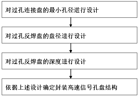
[0023] This embodiment relates to a method for optimizing the design of vias for packaging high-speed signals, such as figure 1 shown, including:

[0024] (1) Design the minimum aperture of the via land;

[0025] (2) Design the diameter of the via anti-pad;

[0026] (3) Design the depth of the via anti-pad;

[0027] (4) According to ...


PUM


Abstract

The invention discloses an optimal design method for a packaging high-speed signal via hole, which comprises the following steps of: (1) designing the minimum hole diameter of a via hole connecting disc, (2) designing the diameter of the via hole anti-bonding pad, (3) designing the depth of the via hole anti-bonding pad, and (4) determining the structure of the packaging high-speed signal hole disc according to the design. The method aims at the impedance discontinuity characteristic of the BGA bonding pad position of a packaging pin, the multi-dimensional parameters such as via hole connecting disc diameter, the via hole anti disc diameter and the via hole anti disc depth are integrated for via hole impedance scanning, a packaging high-speed signal hole disc structure is optimized and determined, the packaging high-speed signal via hole impedance can be effectively improved, return loss of the packaging high-speed signal is reduced, and the transmission characteristics of the packaging high-speed signal are improved.

Description

technical field [0001] The invention belongs to the technical field of integrated circuit chip packaging, and in particular relates to an optimization design method for packaging high-speed signal via holes. Background technique [0002] VLSI (Very Large Scale Integration Circuit, VLSI) is an integrated circuit that combines a large number of transistors into a single chip, and its integration is greater than that of large scale integrated circuits. With the continuous improvement of integration, operating frequency, and computing performance of VLSI chips, the power consumption required for chip operation is also gradually increasing. At the same time, the operating voltage of the chip continues to decrease with the progress of the process, resulting in a decrease in the tolerance of the operating voltage of the chip. In order to ensure the stable and reliable operation of the chip, the power distribution system is facing severe challenges. [0003] Chip packaging is the s...

Claims


Application Information

Patent Timeline
Patent Type & Authority Applications(China)
IPC IPC(8): H01L21/48H01L21/768
CPCH01L21/4814H01L21/4885H01L21/76897H01L21/76898
Inventor 胡晋金利峰郑浩王彦辉李川张弓
Owner JIANGNAN INST OF COMPUTING TECH
Why Eureka
Try Eureka