Substrate and preparation method thereof and display device

A substrate and unified technology, applied in the fields of display devices, substrates and their preparation methods, capable of solving problems such as substrate deformation

Active Publication Date: 2020-01-10
FUZHOU BOE OPTOELECTRONICS TECH CO LTD +1
View PDF4 Cites 0 Cited by
  • Summary
  • Abstract
  • Description
  • Claims
  • Application Information

AI Technical Summary

Problems solved by technology

[0005] Embodiments of the present invention provide a substrate, its preparation method, and a display device, which can improve the problem of deformation of the substrate due to excessive superimposed stress of the texture identification unit and the insulating layer

Method used


Image

  • Substrate and preparation method thereof and display device
  • Substrate and preparation method thereof and display device
  • Substrate and preparation method thereof and display device

Examples


Embodiment Construction

[0041] The following will clearly and completely describe the technical solutions in the embodiments of the present invention with reference to the accompanying drawings in the embodiments of the present invention. Obviously, the described embodiments are only some, not all, embodiments of the present invention. Based on the embodiments of the present invention, all other embodiments obtained by persons of ordinary skill in the art without making creative efforts belong to the protection scope of the present invention.

[0042] The display device can be used as a mobile phone, a tablet computer, a personal digital assistant (personal digital assistant, PDA), a vehicle-mounted computer, etc. The embodiment of the present invention does not specifically limit the specific application of the display device.

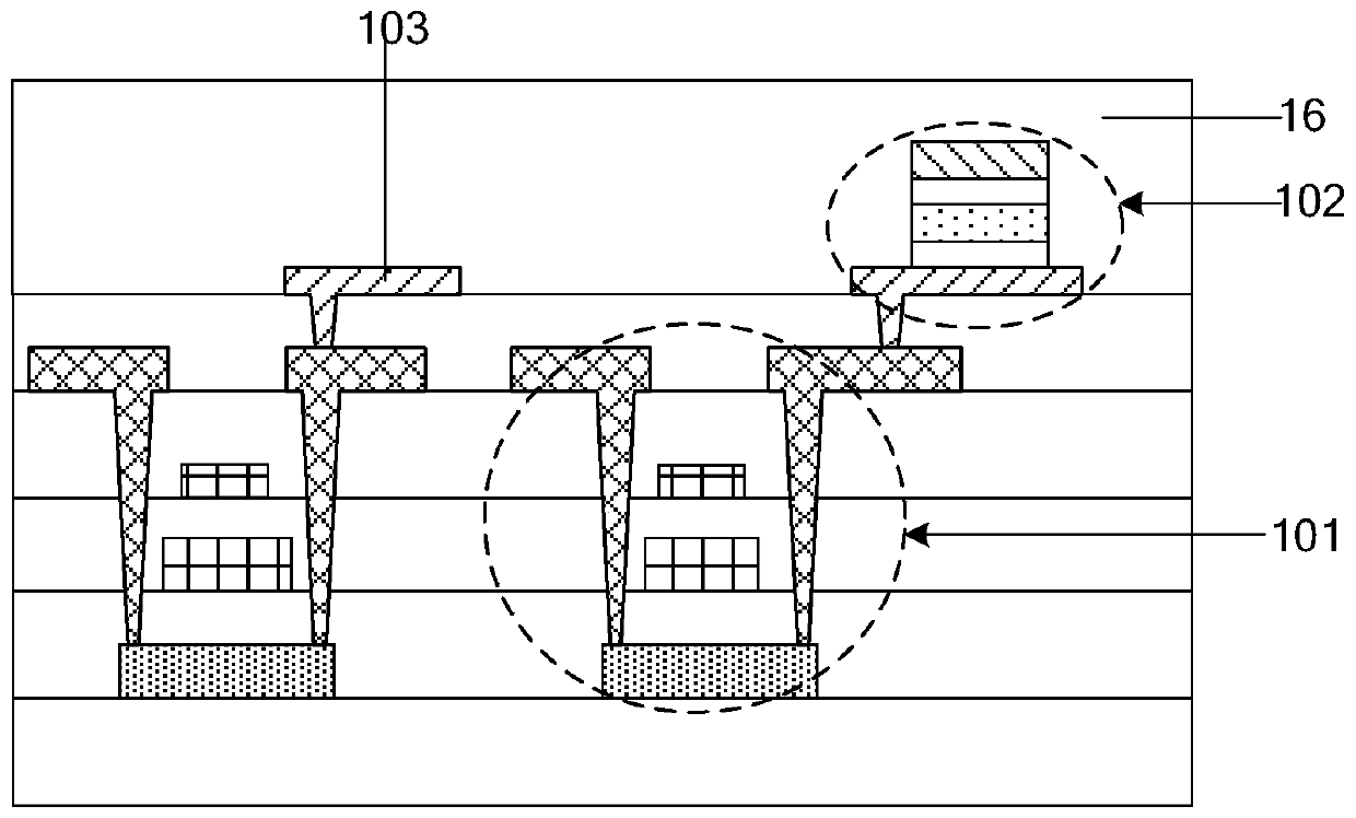
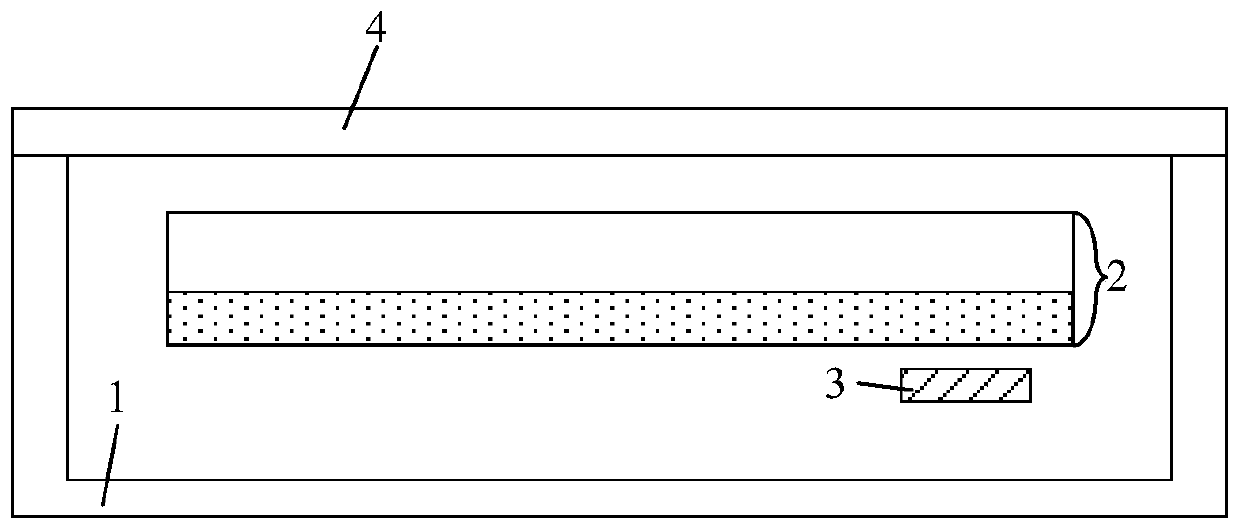
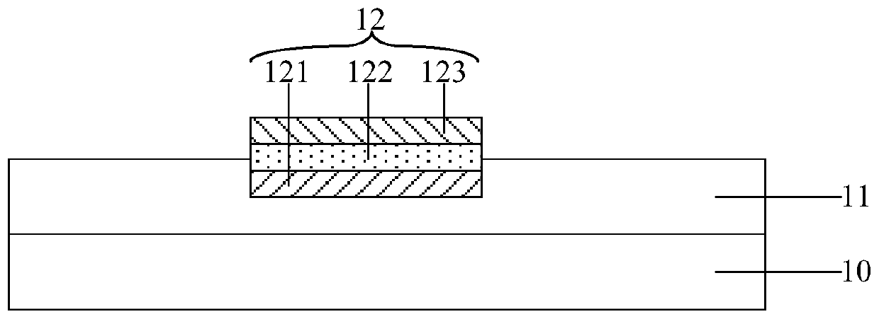
[0043] Such as figure 2 As shown, the display device may include, for example, a frame 1 , a display panel 2 , a circuit board 3 , a cover 4 , and other electronic accessor...


PUM

PropertyMeasurementUnit
thicknessaaaaaaaaaa

Abstract

An embodiment of the invention provides a substrate and a preparation method thereof and a display device, relates to the technical field of display, and can solve the problem of substrate deformationcaused by overlarge superimposition stress of a line recognition unit and an insulating layer. The substrate comprises a substrate body, the insulating layer and the line recognition unit, wherein the insulating layer and the line recognition unit are arranged on the substrate body. The insulating layer is provided with a groove; and at least one part of the line recognition unit is located in the groove.

Description

technical field [0001] The invention relates to the field of display technology, in particular to a substrate, a preparation method thereof, and a display device. Background technique [0002] Currently, the fingerprint recognition function has become an essential part of mobile phones. Among them, under-screen fingerprint recognition is a hot topic in current research. [0003] Such as figure 1 As shown, in the prior art, an optical sensor 102 is provided in the display device to enable the display device to realize the fingerprint recognition function. [0004] However, since the optical sensor 102 and the thin film transistor 101 used to control the operation of the optical sensor 102 have many stacked layers, the stress on the optical sensor 102 and the thin film transistor 101 is too large, which easily leads to deformation or even breakage of the display device. Contents of the invention [0005] Embodiments of the present invention provide a substrate, a manufact...

Claims


Application Information

Patent Timeline
Patent Type & Authority Applications(China)
IPC IPC(8): H01L27/32H01L27/12H01L27/15H01L21/77
CPCH01L27/1248H01L27/1259H01L27/156H10K59/60H10K59/124H01L27/124H01L27/14621H01L27/14683H01L27/14636H01L27/14618H10K59/65H01L27/1222H01L27/1251H01L27/1255H01L27/127
Inventor 庄子华王利忠
Owner FUZHOU BOE OPTOELECTRONICS TECH CO LTD
Why Eureka
Try Eureka