Digital microfluidic system

A digital micro and microfluidic chip technology, applied in the field of microfluidics, can solve the problems of complex microfluidic chip packaging process, small grounding electrodes, etc.

Inactive Publication Date: 2020-01-14
FOSHAN ACXEL BOXIN TECH CO LTD
View PDF6 Cites 9 Cited by
  • Summary
  • Abstract
  • Description
  • Claims
  • Application Information

AI Technical Summary

Problems solved by technology

[0007] In view of this, the embodiment of the present application provides a microfluidic chip with a top cover and a microfluidic chip without a top cover to solve the problem in the prior art that the top cover needs to be electrically conductive in a

Method used


Image

  • Digital microfluidic system
  • Digital microfluidic system
  • Digital microfluidic system

Examples


Embodiment Construction

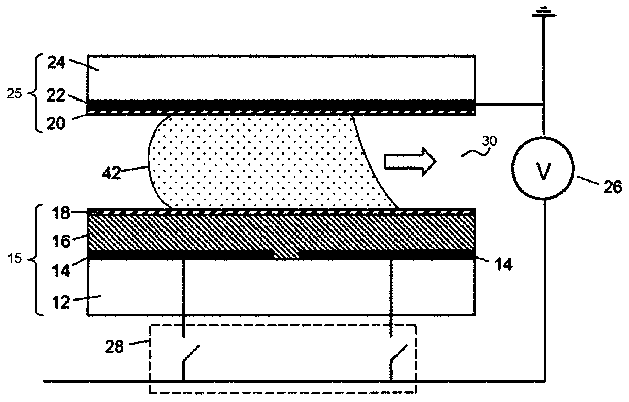
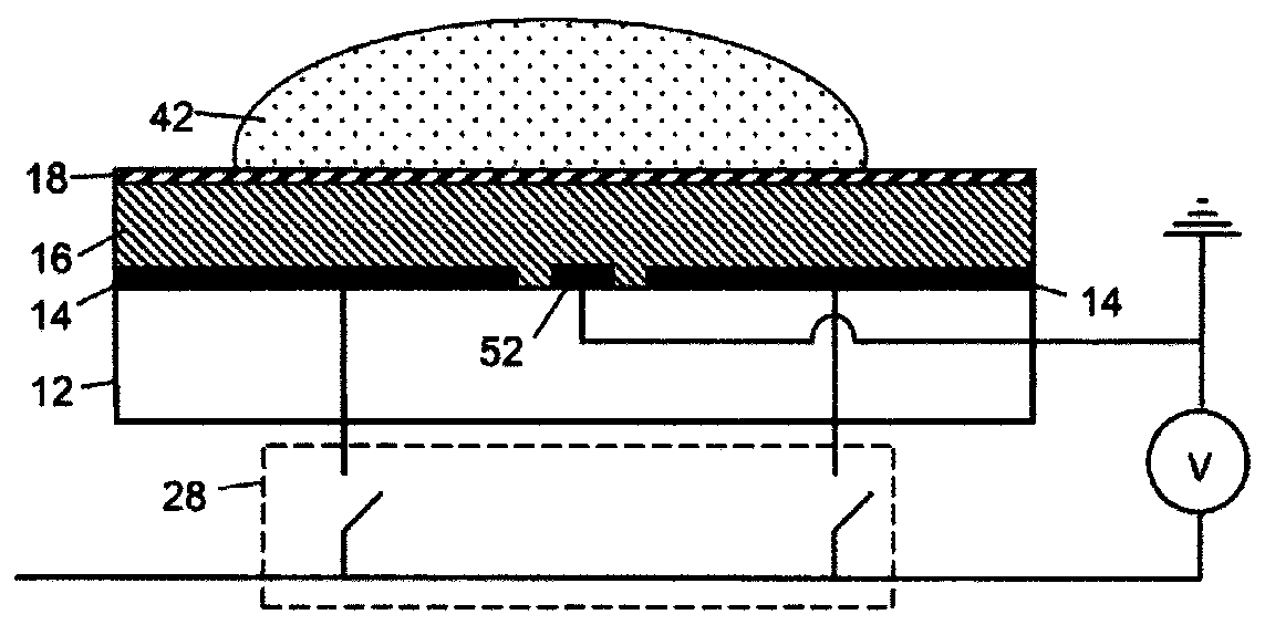
[0031] In order to enable those skilled in the art to better understand the solution of the application, the technical solution in the embodiment of the application will be clearly described below in conjunction with the drawings in the embodiment of the application. Obviously, the described embodiment is the All the way to the embodiment, but not all of the embodiments. Based on the embodiments in this application, all other embodiments obtained by persons of ordinary skill in the art without creative efforts shall fall within the scope of protection of this application.

[0032] The terms "comprising" and any variations thereof in the specification and claims of the present application and the above drawings are intended to cover non-exclusive inclusion. For example, a process, method or system, product or device comprising a series of steps or units is not limited to the listed steps or units, but optionally also includes steps or units not listed, or optionally further inc...


PUM


Abstract

The invention belongs to the technical field of microfluidics, and provides a digital microfluidic system. The digital microfluidic system includes a microfluidic chip and a control circuit, wherein the microfluidic chip includes a bottom electrode plate, the bottom electrode plate includes a plurality of electrodes, and the control circuit is used for separately controlling each electrode to be grounded or powered on and achieving the total area of the grounded electrodes at least five times the total area of the powered electrodes. Therefore, an electric potential difference capable of driving droplets can be formed sufficiently, and the electrodes can be controlled to be grounded through switches without grounding of a top cover or arrangement of a small grounding electrode in the bottom electrode array, so that the packaging difficulty of the digital microfluidic system is reduced.

Description

technical field [0001] The present application belongs to the field of microfluidic technology, and in particular relates to a digital microfluidic system. Background technique [0002] In patent EP3210010B1, two structures of digital microfluidic systems are introduced. [0003] figure 1 Shown is a cross-sectional structure of a digital microfluidic system with a top cover in it. The digital microfluidic system with a top cover includes a top cover 25, a bottom electrode plate 15 and a control circuit. The top cover 25 includes a substrate 24, a conductive layer 22, and a hydrophobic layer 20 connected in sequence, and the bottom electrode plate 15 includes a hydrophobic layer 18, a dielectric layer 16, and a substrate 12 connected in sequence, and is embedded between the dielectric layer 16 and the substrate 12. Between the electrode array 14 (including a plurality of electrodes). A droplet moving space 30 is formed between the hydrophobic layer 20 and the hydrophobic ...

Claims


Application Information

Patent Timeline
IPC IPC(8): B01L3/00
CPCB01L3/50273B01L2400/0415
Inventor 马汉彬苏阳
Owner FOSHAN ACXEL BOXIN TECH CO LTD
Why Eureka
Try Eureka