Array substrate and data line breakpoint repair method there of and display device

A technology for array substrates and data lines, which is applied in the field of display devices and array substrates, can solve problems such as the difficulty of repairing data line breakpoints, and achieve the effect of reducing space and simplifying the film layer structure

Inactive Publication Date: 2020-01-14
WUHAN CHINA STAR OPTOELECTRONICS SEMICON DISPLAY TECH CO LTD
View PDF7 Cites 2 Cited by
  • Summary
  • Abstract
  • Description
  • Claims
  • Application Information

AI Technical Summary

Problems solved by technology

[0005] The embodiments of the present disclosure provide an array substrate, its data line breakpoint repairing method, and a display device, which are used to solve the problem of difficulty in repairing breakpoints in the data lines in the pixel compensation circuit of the existing array substrate

Method used


Image

  • Array substrate and data line breakpoint repair method there of and display device
  • Array substrate and data line breakpoint repair method there of and display device
  • Array substrate and data line breakpoint repair method there of and display device

Examples


Embodiment 1

[0028] Embodiments of the present disclosure provide an array substrate, which is combined below figure 1 Explain in detail.

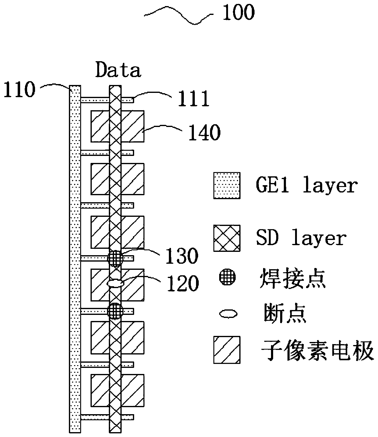
[0029] like figure 1 shown, figure 1 It is a schematic structural diagram of an array substrate 100 provided in an embodiment of the present disclosure. The array substrate 100 includes a base substrate (not shown in the figure), a first metal layer GE1 and a source that are sequentially stacked on the base substrate. Drain electrode layer SD. Wherein, a plurality of data lines Data are arranged in the source-drain electrode layer SD, a plurality of repair lines 100 are arranged in the first metal layer GE1 at intervals, and at least two repairers are arranged on the repair lines 100 at intervals. Line segment 111, the repair sub-line segment 111 extends from the repair line 110 to the projection position of the data line Data on the first metal layer GE1 along the thickness direction of the array substrate, and is insulated from the data line Data ...

Embodiment 2

[0038] Embodiments of the present disclosure provide an array substrate, which is combined below image 3 Explain in detail.

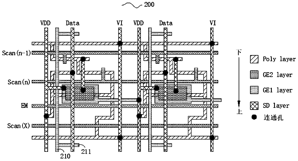
[0039] like image 3 shown, image 3 It is a schematic structural diagram of an array substrate 200 provided by an embodiment of the present disclosure. The array substrate 200 includes a base substrate (not shown in the figure) and is formed on the base substrate as shown in the figure. image 3 The 7T1C pixel compensation circuit shown, image 3 Only the nth stage of the pixel compensation circuit is described. The pixel compensation circuit includes a plurality of data lines Data and repair lines 210 arranged at intervals. At least two repair sub-line segments 211 are arranged on the repair lines 210 at intervals. The repair sub-line segment 211 extends from the repair line 210 to the projection position of the data line Data on the first metal layer GE1 along the thickness direction of the array substrate, and is insulated from the data line Dat...

Embodiment 3

[0051] Embodiments of the present disclosure further provide a method for repairing data line breakpoints on an array substrate, which is applied to the array substrate provided by the above-mentioned embodiments. figure 1 and Figure 4 Explain in detail. like Figure 4 shown, Figure 4 It is a schematic flowchart of a method for repairing a data line breakpoint of an array substrate according to an embodiment of the present disclosure, and the method includes:

[0052] Step S10: Find the position of the breakpoint of the data line;

[0053] Step S20: Connect the repair sub-line segments located at both ends of the breakpoint on the repair line to the two ends of the breakpoint respectively, so that the data line is in a conducting state.

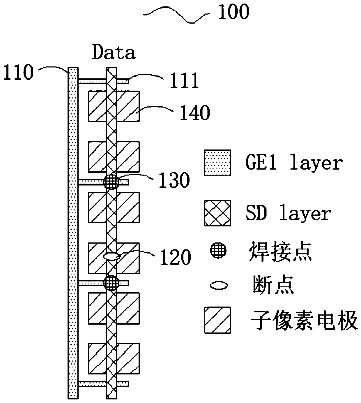
[0054] In this embodiment, when a breakpoint 120 occurs in the data line Data of the array substrate 100 , the breakpoint 120 is found at a specific position of the data line Data. The repair line 110 is provided with a plurality of re...


PUM


Abstract

The invention provides an array substrate and a data line breakpoint repair method thereof and a display device. The array substrate comprises an underlying substrate and a first metal layer and a source and drain electrode layer which are sequentially stacked on the underlying substrate. A plurality of data lines are arranged at intervals in the source and drain electrode layer. A plurality of repair lines are spaced in the first metal layer. At least two repair sub-line segments are spaced on the repair lines. The repair sub-line segments extend from the repair lines to the projection position of the data lines on the first metal layer in the thickness direction of the array substrate and insulated from the data lines.The repair sub-line segmentsare connected with the two ends of the breakpoint when the breakpoint of the data lines occurs so as to complete the repair of the breakpoint of the data lines. Meanwhile, the repair linesare arranged on the first metal layer so that the space of the array substrate occupied by the repair lines is reduced and the film layer structure of the array substrate is simplified.

Description

technical field [0001] The present invention relates to the field of display technology, and in particular, to an array substrate, a method for repairing breakpoints of data lines thereof, and a display device. Background technique [0002] Active-matrix organic light-emitting diodes (AMOLEDs) have developed rapidly because of their unique advantages. The array substrate used for AMOLED is mainly Low Temperature Poly-silicon (LTPS) array substrate. During the production process of LTPS array substrate, it is difficult to ensure the uniformity of the formed large-area polycrystalline silicon semiconductor, which is embodied in the threshold voltage drift. . In order to solve the problem of poor homogeneity of AMOLED LTPS polysilicon, the sub-pixel drive circuit of AMOLED LTPS array substrate needs to use a pixel compensation circuit to offset the influence of threshold voltage drift. [0003] The current mainstream pixel compensation circuit is designed for 7T1C. In order t...

Claims


Application Information

Patent Timeline
Patent Type & Authority Applications(China)
IPC IPC(8): H01L27/12H01L21/66
CPCH01L27/1244H01L22/22H01L27/124H10K59/131H10K71/861H10K71/00
Inventor 张乐
Owner WUHAN CHINA STAR OPTOELECTRONICS SEMICON DISPLAY TECH CO LTD
Why Eureka
Try Eureka