Electromagnetic shielding film, circuit board and preparation method of electromagnetic shielding film

An electromagnetic shielding film and circuit board technology, applied in the field of electronics, can solve the problems such as the inability of the shielding layer to conduct grounding, the easy expansion of the adhesive film layer, and the impact on the reliability of the grounding.

Pending Publication Date: 2020-01-14
GUANGZHOU FANGBANG ELECTRONICS
View PDF4 Cites 0 Cited by
  • Summary
  • Abstract
  • Description
  • Claims
  • Application Information

AI Technical Summary

Problems solved by technology

[0004] At present, the electromagnetic shielding film commonly used in existing circuit boards includes a shielding layer and an adhesive film layer containing conductive particles. The shielding layer is connected to the ground layer of the circuit board through the adhesive film layer containing conductive particles. , the adhesive film layer is easy to expand and the conductive particles of the adhesive film layer are pulled apart, so that the shielding layer cannot be grounded through the adhesive film layer and the ground layer of the circuit board, thus affecting the reliability of grounding

Method used


Image

  • Electromagnetic shielding film, circuit board and preparation method of electromagnetic shielding film
  • Electromagnetic shielding film, circuit board and preparation method of electromagnetic shielding film
  • Electromagnetic shielding film, circuit board and preparation method of electromagnetic shielding film

Examples


Embodiment 1

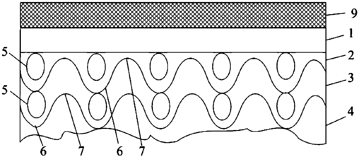
[0041] see figure 1, an electromagnetic shielding film according to a preferred embodiment of the present invention, comprising a first shielding layer 1, N second shielding layers 2, a third shielding layer 3, an adhesive film layer 4 and a plurality of convex particles 5; the first The shielding layer 1, N second shielding layers 2, the third shielding layer 3 and the adhesive film layer 4 are sequentially stacked; the side of the first shielding layer 1 close to the adhesive film layer 4 is flat On the surface, a plurality of convex particles 5 are distributed between the first shielding layer 1 and the second shielding layer 2 and between the second shielding layer 2 and the third shielding layer 3, the The surface of the third shielding layer 3 close to the adhesive film layer 4 is an uneven surface, and the adhesive film layer 4 is disposed on the third shielding layer 3 ; wherein, N is greater than or equal to 1. In this embodiment, N is 1, that is, there is one second...

Embodiment 2

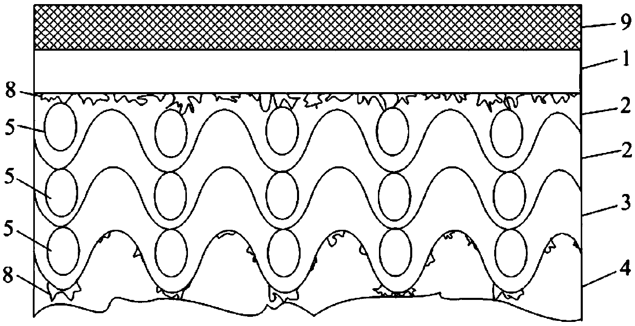
[0057] see figure 2 The difference between the electromagnetic shielding film of this embodiment and Embodiment 1 is that one or more of the second shielding layers 2 in this embodiment are attached with a plurality of said protrusions on the side close to the adhesive film layer 4. Shaped particles5. A plurality of convex particles 5 are attached to one or more of the second shielding layers 2 on the side close to the glue film layer 4, thereby facilitating increasing the proximity of the third shielding layer 3 to the glue. The undulation of one side of the film layer 4 further effectively improves the puncture strength of the third shielding layer 3 . Preferably, one or more of the plurality of convex particles 5 attached to the side of the second shielding layer 2 close to the adhesive film layer 4 are concentrated on the convex portion 6 of the second shielding layer 2 . In this embodiment, N is 2, that is, there are 2 second shielding layers 2 .

[0058] see figure ...

Embodiment 3

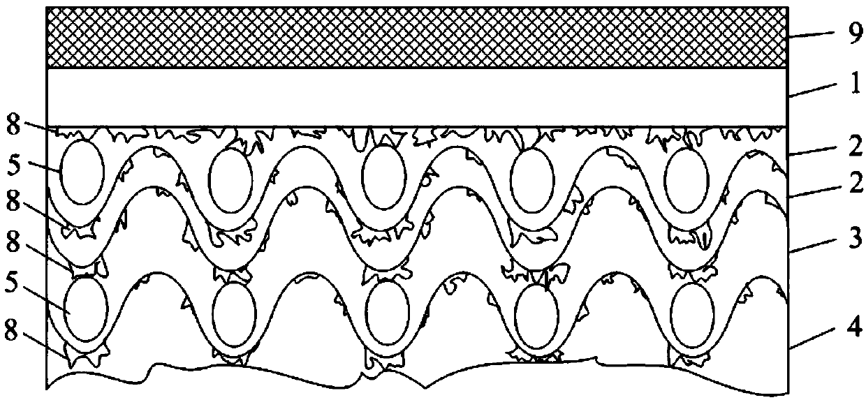
[0065] see image 3 The difference between the electromagnetic shielding film of this embodiment and the second embodiment is that one or more of the second shielding layers 2 in this embodiment are provided with conductive protrusions 8 on the side close to the adhesive film layer 4 . By providing conductive protrusions 8 on one or more of the second shielding layers 2 near the adhesive film layer 4, it is beneficial to increase the distance between the third shielding layer 3 and the adhesive film layer 4. The undulation of one side effectively improves the puncture strength of the third shielding layer 3 . Preferably, one or more conductive protrusions 8 on the side of the second shielding layer 2 close to the adhesive film layer 4 are collectively arranged on the protrusion 6 of the second shielding layer 2 .

[0066] In a specific implementation, the second shielding layer 2 may be formed first, and then the conductive protrusion 8 is formed on the second shielding layer...


PUM

PropertyMeasurementUnit
thicknessaaaaaaaaaa
thicknessaaaaaaaaaa
heightaaaaaaaaaa

Abstract

The invention relates to the technical field of electronics, and discloses an electromagnetic shielding film, a circuit board, and a preparation method of the electromagnetic shielding film. The electromagnetic shielding film comprises a plurality of convex particles, a first shielding layer, N second shielding layers, a third shielding layer, and an adhesive film layer, wherein the first shielding layer, N second shielding layers, the third shielding layer, and the adhesive film layer are successively stacked. The side, which is close to the adhesive film layer, of the first shielding layer is set as a flat surface. The convex particles are distributed between the first shielding layer and the second shielding layer and between the second shielding layer and the third shielding layer. Theside, which is close to the adhesive film layer, of the third shielding layer is a non-flat surface. The non-flat surface of the third shielding layer can pierce the adhesive film layer and is connected with the ground layer of the circuit board when the electromagnetic shielding film is laminated with the circuit board. Ground failure caused by the fact that the conductive particles of the adhesive film layer are pulled apart when the adhesive film layer of the existing electromagnetic shielding film is expanded at high temperature is avoided. The connection of the electromagnetic shieldingfilm and the ground layer of the circuit board is ensured.

Description

technical field [0001] The invention relates to the field of electronic technology, in particular to an electromagnetic shielding film, a circuit board and a preparation method of the electromagnetic shielding film. Background technique [0002] With the rapid development of the electronics industry, electronic products are further developed toward miniaturization, light weight, and high-density assembly, which greatly promotes the development of flexible circuit boards, thereby realizing the integration of component devices and wire connections. Flexible circuit boards can be widely used in industries such as mobile phones, liquid crystal displays, communications and aerospace. [0003] Driven by the international market, functional flexible circuit boards dominate the flexible circuit board market, and an important indicator for evaluating the performance of functional flexible circuit boards is Electromagnetic Interference Shielding (EMI Shielding). With the integration ...

Claims


Application Information

Patent Timeline
Patent Type & Authority Applications(China)
IPC IPC(8): H05K9/00H05K1/02C09J7/29
CPCH05K9/0088H05K1/0218C09J7/29H05K2201/0715C09J2301/16
Inventor 苏陟
Owner GUANGZHOU FANGBANG ELECTRONICS
Why Eureka
Try Eureka