OLED display panel and manufacturing method thereof

A display panel and manufacturing method technology, applied in the direction of electrical components, diodes, electric solid devices, etc., can solve the problems of increasing the luminous efficiency of OLED devices, increasing the encapsulation layer to block water and oxygen pressure, and complicated manufacturing processes, so as to improve the optical effect and bending performance, reducing the risk of luminous efficiency reduction or failure, and optimizing the process flow

Inactive Publication Date: 2020-01-17
WUHAN CHINA STAR OPTOELECTRONICS SEMICON DISPLAY TECH CO LTD
View PDF11 Cites 13 Cited by
  • Summary
  • Abstract
  • Description
  • Claims
  • Application Information

AI Technical Summary

Problems solved by technology

[0005] The OLED display panel and its manufacturing method provided in this disclosure solve the problem of complex manufacturing process when the OLED display panel in the prior art adopts POL-less technology, and the multi-channel wet and baking process will increase the packaging The layer blocks the pressure of water and oxygen, which in turn increases the technical problem of OLED device luminous efficiency reduction or the risk of device failure

Method used


Image

  • OLED display panel and manufacturing method thereof
  • OLED display panel and manufacturing method thereof
  • OLED display panel and manufacturing method thereof

Examples


Embodiment 2

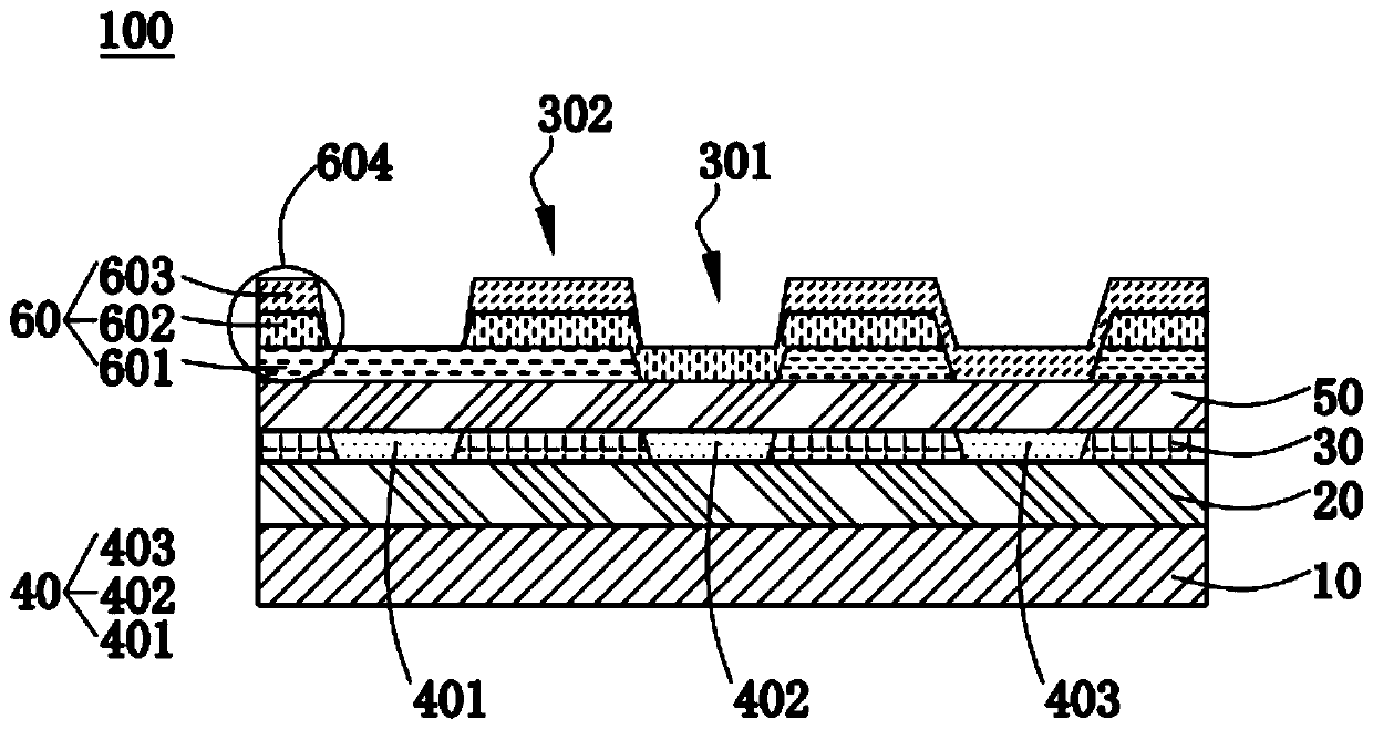
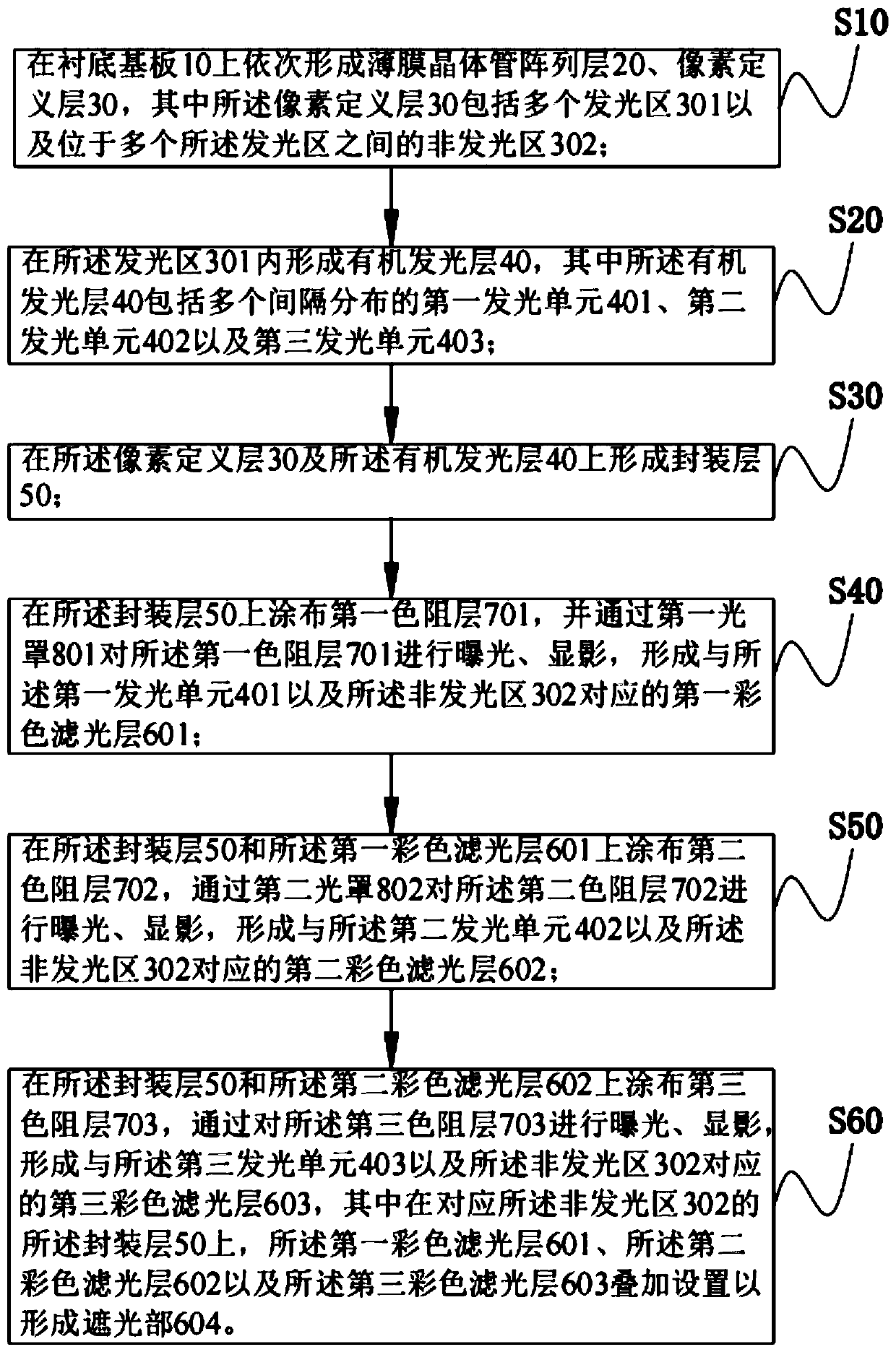
[0056] see figure 2 First of all, it needs to be explained that the embodiment of the present disclosure takes the first color filter layer 601, the second color filter layer 602, and the third color filter layer 603 as an example for illustration and description. Yes, but the embodiments of the present disclosure should not be limited thereto. The manufacturing method of the OLED display panel 100 provided by the disclosed embodiment includes the following steps:

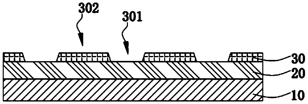
[0057] S10: sequentially forming a thin film transistor array layer 20 and a pixel definition layer 30 on the base substrate 10, wherein the pixel definition layer 30 includes a plurality of light-emitting regions 301 and non-light-emitting regions 302 between the plurality of light-emitting regions;

[0058] Specifically, please refer to image 3 , providing a base substrate 10, the material of the base substrate 10 is PI, the thin film transistor array layer 20 is formed on the base substrate 10, and the thin ...


PUM


Abstract

The invention provides an OLED display panel and a manufacturing method thereof. The OLED display panel comprises a substrate, a thin film transistor array layer, a pixel definition layer, an organiclight-emitting layer, a packaging layer and a color film layer, the color film layer comprises a first color filter layer, a second color filter layer and a third color filter layer. The first color filter layer, the second color filter layer and the third color filter layer are sequentially stacked to form a shading part to replace a black matrix; process flow is optimized, cost of the productionequipment, the photomask and the material is greatly reduced, the risk that the luminous efficiency of the OLED device is reduced or fails after the photoetching process is reduced, the pixel definition layer also has the shading effect, and the optical effect and the bending performance of the OLED display panel can be further improved by combining the pixel definition layer with the shading part.

Description

technical field [0001] The present disclosure relates to the field of display technology, in particular to an OLED display panel and a manufacturing method thereof. Background technique [0002] Adding a polarizer (polarizer, POL) to the display panel can effectively reduce the reflectivity of the display panel under strong light, but it also has the following defects. On the one hand, the polarizer loses nearly 58% of the light output, especially for Organic Light-Emitting Diode (OLED) display panels, which greatly increases its life burden; on the other hand, due to the large thickness of the polarizer 1. The material is brittle, which is not conducive to the development of dynamic bending products. In order to develop dynamic bending products based on OLED display technology, new materials, new technologies and new processes must be introduced to replace polarizers. [0003] The technology of using color filter instead of polarizer is classified as POL-less technology, i...

Claims


Application Information

Patent Timeline
Patent Type & Authority Applications(China)
IPC IPC(8): H01L27/32
CPCH10K59/35H10K59/38H10K59/126H10K59/122H10K59/12H10K59/1201H10K50/865H10K50/844H10K50/84H10K59/1213H10K71/00
Inventor 黄晓雯王雷龚文亮鲜于文旭
Owner WUHAN CHINA STAR OPTOELECTRONICS SEMICON DISPLAY TECH CO LTD
Why Eureka
Try Eureka