Manufacturing method of circuit board and circuit board

A manufacturing method and circuit board technology, which can be used in multilayer circuit manufacturing, printed circuit manufacturing, printed circuit and other directions, and can solve the problems of insufficient precision of circuit boards and rough side walls.

Inactive Publication Date: 2020-01-17
PEKING UNIV FOUNDER GRP CO LTD +1
View PDF4 Cites 0 Cited by
  • Summary
  • Abstract
  • Description
  • Claims
  • Application Information

AI Technical Summary

Problems solved by technology

[0005] A method for manufacturing a circuit board and a circuit board provided by the present invention are used to solve the technical problem that the side wall of the stepped groove formed by cutting with a milling cutter is relatively rough, resulting in insufficient precision of the circuit board

Method used


Image

  • Manufacturing method of circuit board and circuit board
  • Manufacturing method of circuit board and circuit board
  • Manufacturing method of circuit board and circuit board

Examples


Embodiment Construction

[0043] Reference will now be made in detail to the exemplary embodiments, examples of which are illustrated in the accompanying drawings. When the following description refers to the accompanying drawings, the same numerals in different drawings refer to the same or similar elements unless otherwise indicated. The implementations described in the following exemplary examples do not represent all implementations consistent with the present disclosure. Rather, they are merely examples of apparatuses and methods consistent with aspects of the present disclosure as recited in the appended claims.

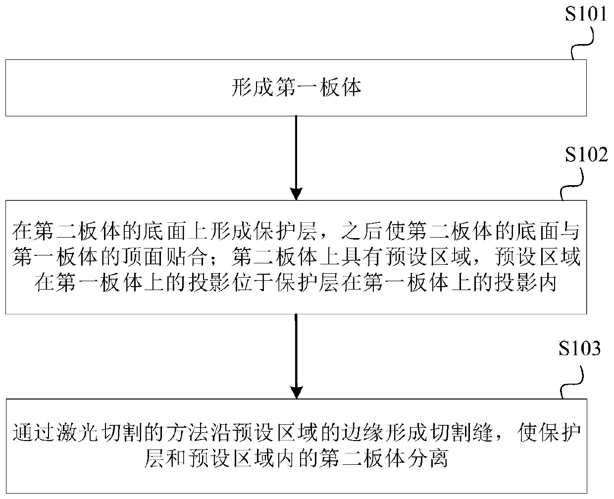
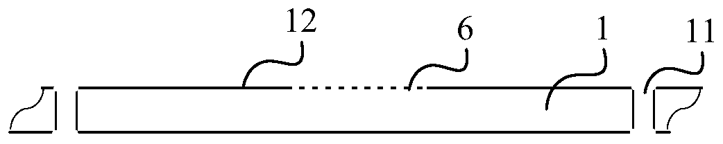
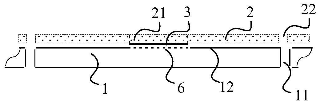
[0044] figure 1 A flowchart of a method for manufacturing a circuit board provided by an embodiment of the present invention; figure 2 A schematic diagram after forming a circuit pattern and a first through hole on the top surface of the first board in the method for manufacturing a circuit board provided by an embodiment of the present invention; image 3 It is a schematic diagram ...


PUM


Abstract

The invention provides a manufacturing method of a circuit board and the circuit board. The manufacturing method comprises the following steps of forming a first board body; forming a protective layeron the bottom surface of a second plate body, and then attaching the bottom surface of the second plate body to the top surface of the first plate body, wherein the second plate body is provided witha preset area, and the projection of the preset area on the first plate body is located in the projection of the protective layer on the first plate body; forming a cutting seam along the edge of thepreset area through a laser cutting method, so that the protective layer, the second plate body in the preset area and the first plate body are separated. By forming the protective layer between thefirst plate body and the second plate body, and forming the cutting seam along the edge of the preset area through the laser cutting method, the protective layer and the second plate body in the preset area can be separated from the first plate body, compared with a stepped groove formed by a milling mode, the side wall of the formed stepped groove is more smoother, and further the precision of the formed circuit board is high.

Description

technical field [0001] The invention relates to the field of electronic equipment manufacturing, in particular to a method for manufacturing a circuit board and the circuit board. Background technique [0002] With the continuous development of electronic communication technology, the requirements for circuit board space are getting higher and higher. In order to reduce the space occupied by the circuit board, a stepped groove (English name Cavity) is generally provided on the circuit board, and at least part of the electronic devices are installed in the stepped groove, so as to prevent the electronic device from being exposed to the outside of the circuit board and occupying too much space. Therefore, how to form stepped grooves on circuit boards has become a research hotspot. [0003] In related technologies, step grooves are often formed by cutting. Specifically, a milling cutter is used to cut in a predetermined area on the circuit board to remove material in the prese...

Claims


Application Information

Patent Timeline
Patent Type & Authority Applications(China)
IPC IPC(8): H05K3/46H05K1/18H05K1/02
CPCH05K1/02H05K1/185H05K3/4697
Inventor 金立奎车世民陈德福王细心雷刚
Owner PEKING UNIV FOUNDER GRP CO LTD
Why Eureka
Try Eureka