Wafer center calibration method and device

A wafer and center technology, applied in the field of wafer calibration, can solve problems such as low detection efficiency and wafer center error, and achieve the effect of improving efficiency and avoiding errors

Active Publication Date: 2020-01-24
福建省福联集成电路有限公司
View PDF7 Cites 1 Cited by
  • Summary
  • Abstract
  • Description
  • Claims
  • Application Information

AI Technical Summary

Problems solved by technology

[0003] For this reason, it is necessary to provide a wafer center calibration device, which is used to solve the technical problems of manual naked eye calibration of wafer center errors and low detection efficiency.

Method used


Image

  • Wafer center calibration method and device
  • Wafer center calibration method and device
  • Wafer center calibration method and device

Examples


Embodiment Construction

[0040] In order to explain in detail the technical content, structural features, achieved goals and effects of the technical solution, the following will be described in detail in conjunction with specific embodiments and accompanying drawings.

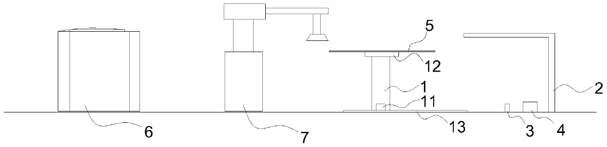
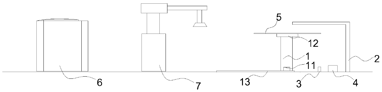
[0041] see figure 1 , is a schematic structural diagram of a wafer center calibration device related to a specific embodiment of the present invention.

[0042] The device for calibrating the center of the wafer includes a stage 1 , a block 2 , a distance measuring sensor 3 and a controller 4 . The top surface of the stage 1 is higher than the distance measuring sensor 3 , the distance measuring sensor 3 is arranged on one side of the stage, and the blocking platform 2 is located directly above the distance measuring sensor 3 . Preferably, the stop includes a horizontal platform and a vertical column supporting the horizontal platform, and the location of the stop directly above the distance measuring sensor means that the horizontal...


PUM


Abstract

The invention relates to a wafer center calibration device. The wafer center calibration device comprises a carrying platform, a blocking platform, a distance measuring sensor and a controller; the top surface of the carrying table is higher than the distance measuring sensor; the distance measuring sensor is arranged on one side of the carrying table; the blocking platform is located over the distance measuring sensor; the carrying platform is used for carrying a wafer and driving the wafer to move; the distance measuring sensor is used for acquiring horizontal distance information and vertical distance information; and the controller is connected with the distance measuring sensor and is used for controlling the carrying platform to rotate by a preset angle or controlling the carrying platform to move close to or away from the distance measuring sensor. According to the wafer center calibration device of the invention, the controller is used for processing the information of the distance measuring sensor and judging a wafer of which the center position deviates. With the wafer center calibration device adopted, the wafer of which the center position deviates can be rapidly screened out; the center calibration efficiency of the wafer is improved; and errors of manual detection are effectively avoided.

Description

technical field [0001] The invention relates to the field of wafer calibration, in particular to a method and device for wafer center calibration. Background technique [0002] In recent years, whether the placement of the center of the wafer is accurate or not is usually calibrated by human eyes. However, there will be visual errors due to manual calibration, and an additional process is required for wafer edge detection during manual calibration. At the same time, the existing machine will not only stop the operation of the current wafer, but also stop the operation of the remaining wafers due to problems such as the center of the wafer is not calibrated or the edge is found, which greatly affects the work efficiency. Contents of the invention [0003] Therefore, it is necessary to provide a wafer center calibration device, which is used to solve the technical problems of manual naked eye calibration of wafer center errors and low detection efficiency. [0004] In orde...

Claims


Application Information

Patent Timeline
Patent Type & Authority Applications(China)
IPC IPC(8): H01L21/68
CPCH01L21/68
Inventor 马跃辉黄光伟李立中林伟铭陈智广吴淑芳庄永淳吴靖
Owner 福建省福联集成电路有限公司
Why Eureka
Try Eureka