Gallium nitride MOSFET packaging stress-strain distribution sensing structure

A technology for packaging stress and strain distribution, which is applied in the measurement of electric/magnetic solid deformation, the measurement of the property and force of applied piezoelectric resistance materials, and electromagnetic measurement devices. It can solve the problem that the structure of GaN MOSFET chips varies greatly and cannot be accurately Reflect the actual situation of the GaN MOSFET chip functional structure and the influence of electrical characteristics, etc., to achieve the effect of simple and easy detection method and process, simple and easy preparation process, and compatibility between preparation process and packaging process

Pending Publication Date: 2020-01-31
YANGZHOU YANGJIE ELECTRONIC TECH CO LTD
View PDF1 Cites 0 Cited by
  • Summary
  • Abstract
  • Description
  • Claims
  • Application Information

AI Technical Summary

Problems solved by technology

However, the problem with the above test method is that the structure of this dedicated stress-strain test chip is very different from that of the actual GaN MOSFET chip, and cannot accurately reflect the actual conditions and conditions of stress and strain distribution on the GaN MOSFET chip in the package. Its influence on the functional structure and electrical characteristics of GaN MOSFET chips

Method used


Image

  • Gallium nitride MOSFET packaging stress-strain distribution sensing structure
  • Gallium nitride MOSFET packaging stress-strain distribution sensing structure
  • Gallium nitride MOSFET packaging stress-strain distribution sensing structure

Examples


Embodiment Construction

[0040] The present invention will be further described below in conjunction with the accompanying drawings and embodiments.

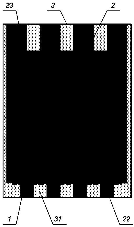
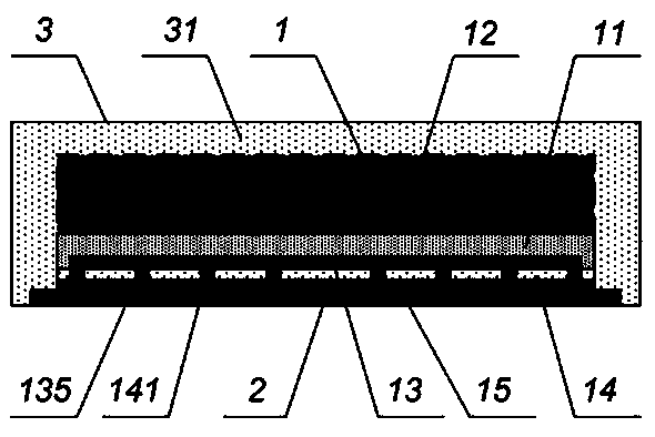
[0041] The present invention includes a chip 1, a lead frame 2, and an encapsulation layer 31 covering the chip and the lead frame,

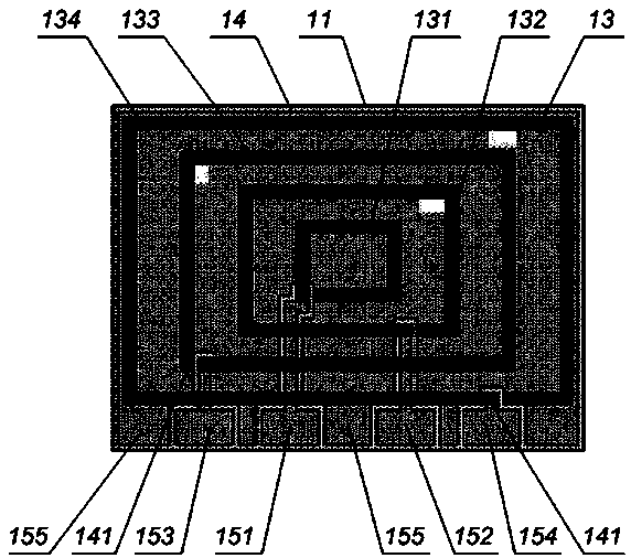
[0042] The chip includes a substrate 11, a gallium nitride MOSFET structure layer 12 fabricated on the substrate, a piezoresistor 13 fabricated on the bottom of the substrate, an insulating layer 14 covering the bottom surface of the substrate, and electrodes fabricated on the insulating layer layer 15,

[0043] The piezoresistor 13 includes at least two piezoresistive rings nested sequentially from the inside to the outside, wherein the odd-numbered piezoresistive rings have a gap one in the lower part, and the even-numbered piezoresistive rings have a gap two in the lower part. The gaps 1 and 2 are arranged in a staggered manner, and the horizontal spacing and the vertical spacing between adjacent piezoresistive rings ...


PUM


Abstract

The invention relates to a gallium nitride MOSFET packaging stress-strain distribution sensing structure. The invention relates to the technical field of power semiconductor devices, in particular toa gallium nitride MOSFET packaging stress-strain distribution sensing structure. The gallium nitride MOSFET packaging stress-strain distribution sensing structure provided by the invention is convenient to process and improves the detection reliability. The sensing structure comprises a chip, a lead frame and a packaging layer covering the chip and the lead frame, the chip comprises a substrate, agallium nitride MOSFET structure layer manufactured on the substrate, a piezoresistor manufactured at the bottom of the substrate, an insulating layer covering the bottom surface of the substrate andan electrode layer manufactured on the insulating layer, and the substrate is made of monocrystalline silicon. The electrode layer is made of gold, and the lead frame is made of copper or copper alloy. The preparation process of the gallium nitride MOSFET packaging stress-strain sensing structure is compatible with the preparation process and the packaging process of a conventional gallium nitride MOSFET chip, and the preparation process is simple and easy to implement.

Description

technical field [0001] The invention relates to the technical field of power semiconductor devices, in particular to a GaN MOSFET packaging stress and strain distribution sensing structure. Background technique [0002] Gallium nitride MOSFET is a type of field effect transistor based on gallium nitride and aluminum gallium nitride. Due to GaN's high breakdown electric field, high saturation velocity, and good temperature characteristics, GaN MOSFETs have broad application prospects in high-power high-frequency energy conversion and high-frequency microwave communications. [0003] Gallium nitride MOSFET devices contain chip materials and packaging materials with different thermal expansion coefficients. Temperature changes during manufacturing and use cause thermal mismatch between materials, resulting in non-uniform distribution of thermal stress and strain at each layer of materials and their interfaces. , leading to changes in the functional structure of the chip, resul...

Claims


Application Information

Patent Timeline
Patent Type & Authority Applications(China)
IPC IPC(8): G01L1/18G01B7/16H01L23/31H01L23/495
CPCG01B7/18G01L1/18H01L23/3107H01L23/495
Inventor 赵成王毅
Owner YANGZHOU YANGJIE ELECTRONIC TECH CO LTD
Why Eureka
Try Eureka