Chip integrated manufacturing auxiliary equipment based on light pressure principle

A kind of auxiliary equipment and principle technology, applied in semiconductor/solid-state device manufacturing, electrical components, circuits, etc., can solve the problems of high positioning accuracy, troublesome transfer, no protection measures, etc.

Inactive Publication Date: 2020-02-28
冯聪
View PDF0 Cites 4 Cited by
  • Summary
  • Abstract
  • Description
  • Claims
  • Application Information

AI Technical Summary

Problems solved by technology

[0003] The manufacturing of the chip is divided into five steps: photolithography, etching, thin film, doping, and chemical mechanical planarization. Among them, photolithography is an extremely important step. The basic process of the photolithography process is: uniform glue, drying, transfer, Positioning, photolithography, baking, etc. Although this process is relatively mature, the transfer step is very troublesome, because the chip is a high-precision component, and the positioning accuracy is very high, and a slight deviation will lose the desired effect. Although the existing lithography equipment

Method used


Image

  • Chip integrated manufacturing auxiliary equipment based on light pressure principle
  • Chip integrated manufacturing auxiliary equipment based on light pressure principle
  • Chip integrated manufacturing auxiliary equipment based on light pressure principle

Examples


Embodiment Construction

[0020] The following will clearly and completely describe the technical solutions in the embodiments of the present invention with reference to the accompanying drawings in the embodiments of the present invention. Obviously, the described embodiments are only some, not all, embodiments of the present invention. Based on the embodiments of the present invention, all other embodiments obtained by persons of ordinary skill in the art without making creative efforts belong to the protection scope of the present invention.

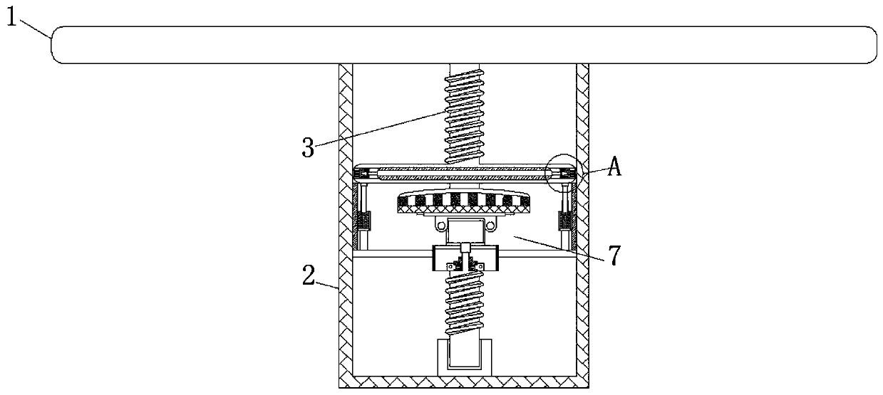
[0021] see Figure 1-4 , an auxiliary device for chip integrated manufacturing based on the principle of light pressure, including a turntable 1, the turntable 1 is designed with a concave surface, and the concave surface is inside the closed box 2, and the curvature of the concave surface will not cause accumulation of photoresist, and the bottom of the turntable 1 is fixed A closed box 2 is movably connected, and the interior of the closed box 2 is movably c...


PUM


Abstract

The invention relates to the technical field of chip manufacturing and discloses chip integrated manufacturing auxiliary equipment based on a light pressure principle. The equipment comprises a rotarydisc, wherein a closed box is fixedly and movably connected with the bottom of the rotary disc, a rotary shaft is movably connected into the closed box, a surface of the rotary shaft is sleeved witha shell, a shading disc is movably connected with a top wall of the interior of the shell, a light pressure mechanism is movably connected with the bottom of the shading disc, adjusting springs are movably connected with two sides of the light pressure mechanism, and the light pressure mechanism comprises a light emitting plate. The limiting spring is pulled to move, a carving plate is in contactwith the shading disc, specific images are formed, after glue uniformizing is completed, the wavelength generated by a light wave box is adjusted, the light emitting plate generates a light source, anadjusting plate and the adjusting springs are moved according to an imaging distance between the carving plate and the rotary disc, an irradiation range of the light emitting plate can be enlarged and shrunk, developing photoetching is conducted on the light emitting plate, and thereby the effect that the photoetching process can be completed through one-time positioning without transferring is achieved.

Description

technical field [0001] The invention relates to the technical field of chip manufacturing, in particular to a chip integrated manufacturing auxiliary device based on the light pressure principle. Background technique [0002] Chip is a general term for semiconductor component products. Chip is also called integrated circuit or microcircuit, microchip, chip / chip: in electronics, it is a way to miniaturize circuits and is often manufactured on the surface of semiconductor wafers. [0003] The manufacturing of the chip is divided into five steps: photolithography, etching, thin film, doping, and chemical mechanical planarization. Among them, photolithography is an extremely important step. The basic process of the photolithography process is: uniform glue, drying, transfer, Positioning, photolithography, baking, etc. Although this process is relatively mature, the transfer step is very troublesome, because the chip is a high-precision component, and the positioning accuracy is ...

Claims


Application Information

Patent Timeline
IPC IPC(8): H01L21/027H01L21/67
CPCH01L21/0274H01L21/6715
Inventor 冯聪
Owner 冯聪
Why Eureka
Try Eureka