Display panel and preparation method thereof

A display panel and substrate technology, which is applied in semiconductor/solid-state device manufacturing, organic semiconductor devices, electric solid-state devices, etc., can solve the problems of poor panel display uniformity and achieve the effect of poor display uniformity

Active Publication Date: 2020-02-28
SHENZHEN CHINA STAR OPTOELECTRONICS SEMICON DISPLAY TECH CO LTD
View PDF4 Cites 7 Cited by
  • Summary
  • Abstract
  • Description
  • Claims
  • Application Information

AI Technical Summary

Problems solved by technology

[0005] The present application provides a display panel and a preparation method thereof, which can solve the problem of poor display uniformity of the existing organic electroluminescent display panel due to voltage drop

Method used


Image

  • Display panel and preparation method thereof
  • Display panel and preparation method thereof
  • Display panel and preparation method thereof

Examples


Embodiment Construction

[0038] The following descriptions of the various embodiments refer to the accompanying drawings to illustrate specific embodiments that the present application can be used to implement. The directional terms mentioned in this application, such as [top], [bottom], [front], [back], [left], [right], [inside], [outside], [side], etc., are for reference only The orientation of the attached schema. Therefore, the directional terms used are used to illustrate and understand the application, but not to limit the application. In the figures, structurally similar elements are denoted by the same reference numerals.

[0039] The present application aims at the problem of poor display uniformity of the existing organic electroluminescent display panel due to voltage drop, and this embodiment can solve this defect.

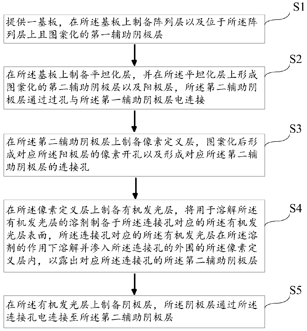
[0040] Such as figure 1 As shown, it is a flow chart of the manufacturing method of the display panel provided by the embodiment of the present application. and refer to ...


PUM


Abstract

The invention provides a display panel and a preparation method thereof. The preparation method comprises the following steps: a pixel definition layer is prepared on a substrate, on which a first auxiliary cathode layer and a second auxiliary cathode layer are formed; the pixel definition layer is patterned to form pixel openings and connection holes corresponding to the second auxiliary cathodelayer; an organic light-emitting layer is prepared on the whole surface of the pixel definition layer, and a solvent is printed on the organic light-emitting layer in the connection holes; the organiclight-emitting layer in the connection holes is dissolved under the action of the solvent, and the solution infiltrates into the pixel definition layer on the periphery of the connection holes, thusexposing the second auxiliary cathode layer corresponding to the connection holes; and the cathode layer can be effectively electrically connected to the second auxiliary cathode layer and the first auxiliary cathode layer through the connection holes. The problem that an existing organic electroluminescent display panel has poor panel display uniformity due to voltage drop is solved in the invention.

Description

technical field [0001] The present application relates to the field of display technology, in particular to a display panel and a manufacturing method thereof. Background technique [0002] Organic electroluminescent display panels have become the development trend of future display technology due to their excellent characteristics such as high contrast ratio, wide color gamut, fast response speed, and flexibility. [0003] Organic electroluminescent display panels are divided into bottom emission and top emission according to the direction of light emission. Due to the design aperture ratio of bottom emission, it cannot meet the high-resolution development needs of market products. Therefore, it is necessary to develop top emission OLED device technology. Top emission OLED design has requirements High resolution, good optical effect of transparent cathode, etc., but the transparent cathode cannot meet the technical requirements at the same time due to the surface resistance...

Claims


Application Information

Patent Timeline
Patent Type & Authority Applications(China)
IPC IPC(8): H01L51/52H01L51/50H01L27/32H01L21/77
CPCH10K59/122H10K50/11H10K50/824H10K59/1201H10K71/00H10K2102/103
Inventor 魏锋李金川
Owner SHENZHEN CHINA STAR OPTOELECTRONICS SEMICON DISPLAY TECH CO LTD
Why Eureka
Try Eureka