A power semiconductor module packaging structure

A power semiconductor and module packaging technology, which is applied in the direction of semiconductor devices, semiconductor/solid-state device components, electric solid-state devices, etc., can solve the problem of power semiconductor module current sharing, heat dissipation, thermal stress, and reliability affecting the reliable use of power semiconductor modules, Reducing the reliability of power semiconductor modules The uniformity of power semiconductor modules and the inability to directly manufacture single-chip chips can achieve the effects of reducing costs, reducing the number of chips, and the number of pins

Active Publication Date: 2021-08-10
ZHUZHOU CRRC TIMES SEMICON CO LTD
View PDF4 Cites 0 Cited by
  • Summary
  • Abstract
  • Description
  • Claims
  • Application Information

AI Technical Summary

Problems solved by technology

[0003] However, since the existing power semiconductor chip manufacturing technology is still unable to directly manufacture single-chip chips to meet the power requirements of users, the use of multi-chip parallel connection has become a typical way to meet high power requirements
However, with the increase in the number of parallel-connected power semiconductor chips, current sharing, heat dissipation, thermal stress, and reliability inside the power semiconductor module have become important challenges that affect the reliable use of power semiconductor modules.
Furthermore, with the increase in the number of power semiconductor chips, the production process of power semiconductor modules requires higher precision and consistency, resulting in increased process complexity
At the same time, the product yield will be affected by the inconsistency and process inconsistency brought about by the excessive number of chips, which reduces the reliability of the entire power semiconductor module and the uniformity between power semiconductor modules

Method used


Image

  • A power semiconductor module packaging structure
  • A power semiconductor module packaging structure
  • A power semiconductor module packaging structure

Examples


Embodiment Construction

[0030]The implementation of the present invention will be described in detail below in conjunction with the accompanying drawings and examples, so as to fully understand and implement the process of how to apply technical means to solve technical problems and achieve technical effects in the present invention. It should be noted that, as long as there is no conflict, each embodiment and each feature in each embodiment of the present invention can be combined with each other, and the formed technical solutions are all within the protection scope of the present invention.

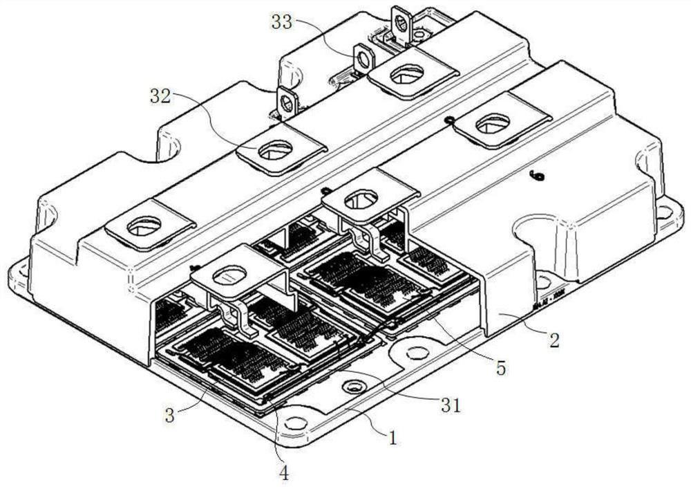
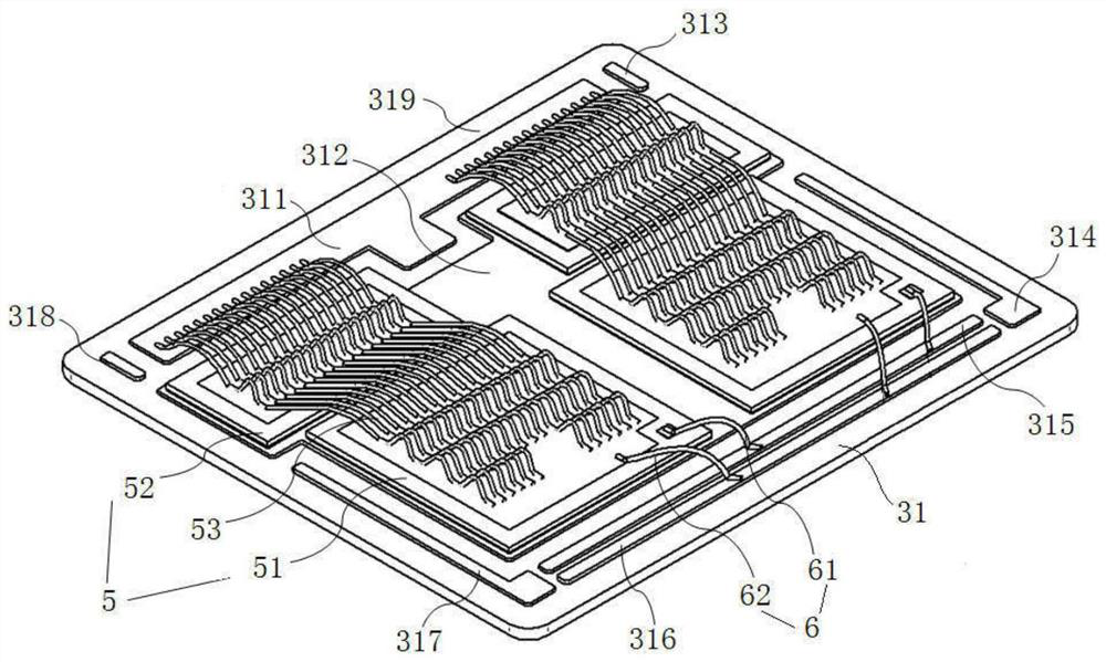
[0031] like figure 1 As shown, the power semiconductor module packaging structure proposed by the present invention includes a substrate 1; a housing 2, which is sealed and fastened to the substrate 1; In the accommodation space, it is used to form a topology control circuit structure. The power semiconductor module subunit 3 includes a plurality of backing plates 31 arranged at intervals on the substrate 1,...


PUM


Abstract

The invention discloses a package structure of a power semiconductor module, which is characterized in that it comprises a substrate; a casing, the casing is fastened to the substrate; and a power semiconductor module subunit is arranged between the casing and the substrate. In the accommodation space formed by the substrate, it is used to form a topology control circuit structure. The power semiconductor module subunit includes a plurality of backing boards arranged at intervals on the substrate, and the main power terminal is passed between the two facing backing boards. It is connected with the module-level bonding wire, and the top of the main power terminal extends out of the top of the housing; the auxiliary terminal is used to introduce the driving signal into the power semiconductor module subunit, and the bottom pin of the auxiliary terminal Connected with the liner, the top of the auxiliary terminal extends out of the top of the housing. The invention can improve the heat dissipation efficiency of the power semiconductor module, balance parasitic inductance or resistance parameters, improve the consistency of the process, have low loss and good reliability.

Description

technical field [0001] The invention relates to a packaging structure of a power semiconductor module, which belongs to the field of semiconductor devices. Background technique [0002] Users of power semiconductor modules expect power modules to be able to increase output power with smaller volume and lower price. The increase in power density poses various challenges for power semiconductor chips and corresponding packaging. For different application scenarios, a variety of new packaging solutions are accompanied by the rapid development of power semiconductor chip technology, packaging materials, packaging processes, and packaging design. [0003] However, since the existing power semiconductor chip manufacturing technology is still unable to directly manufacture single-chip chips to meet the power requirements of users, the parallel connection of multiple chips has become a typical way to meet high power requirements. However, with the increase in the number of paralle...

Claims


Application Information

Patent Timeline
Patent Type & Authority Patents(China)
IPC IPC(8): H01L23/055H01L23/492H01L23/49
CPCH01L23/055H01L23/492H01L24/48H01L2224/48091H01L2224/48137H01L2224/48157H01L2224/49111H01L2224/48139H01L2224/48227H01L2224/0603H01L2224/4846
Inventor 刘国友李道会齐放马修·帕克伍德李想
Owner ZHUZHOU CRRC TIMES SEMICON CO LTD
Why Eureka
Try Eureka