Chip package structure semi-finished product, module, and fabrication method of chip package structure semi-finished product

A technology of chip packaging structure and semi-finished products, which is applied in the fields of semiconductor/solid-state device manufacturing, semiconductor devices, and semiconductor/solid-state device components, etc. It can solve the problems of high manufacturing cost, long time for laying conductive terminals, and cumbersome conductive terminal layout. , to achieve the effect of reducing manufacturing costs and reducing the difficulty of layout

Active Publication Date: 2020-03-10
TARNG YU ENTERPRISE
View PDF7 Cites 2 Cited by
  • Summary
  • Abstract
  • Description
  • Claims
  • Application Information

AI Technical Summary

Problems solved by technology

[0002] In the traditional IC packaging process, the number of conductive terminals is large, which makes the layout of the conductive terminals very cumbersome. It is often necessary to deploy a machine to send each conductive terminal to the circuit substrate one by one for welding, resulting in a long time for the layout of the conductive terminals and lowering the manufacturing cost. stay high
[0003] Therefore, in the IC packaging process, how to reduce the difficulty of laying conductive terminals and solve the problems of long laying time of conductive terminals has become a technical issue that the industry is eager to challenge and overcome.

Method used


Image

  • Chip package structure semi-finished product, module, and fabrication method of chip package structure semi-finished product
  • Chip package structure semi-finished product, module, and fabrication method of chip package structure semi-finished product
  • Chip package structure semi-finished product, module, and fabrication method of chip package structure semi-finished product

Examples


Embodiment Construction

[0056] The following content will be combined with drawings to illustrate the technical content of the application through specific embodiments. Those who are familiar with this technology can easily understand other advantages and effects of the application from the content disclosed in this specification. The present application can also be implemented or applied by other different specific embodiments. Various modifications and changes may be made to the details in this specification based on different viewpoints and applications without departing from the spirit of this application. In particular, the scales and relative positions of various components in the drawings are for exemplary purposes only, and do not represent the actual situation of the implementation of the application.

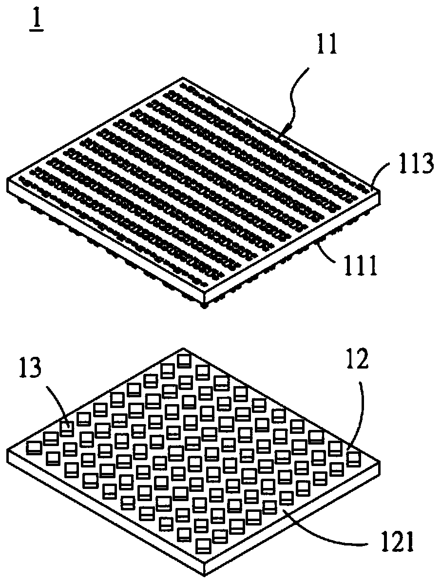
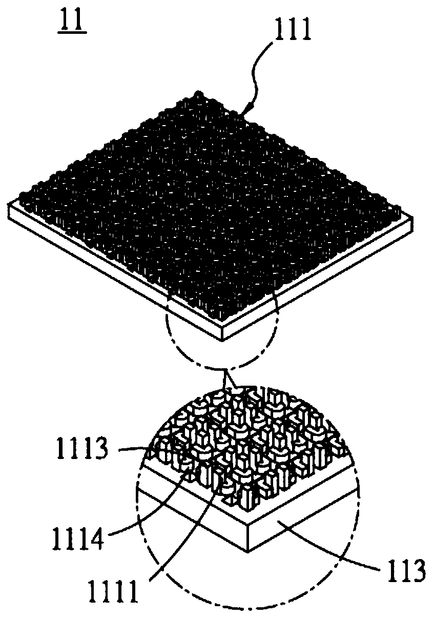
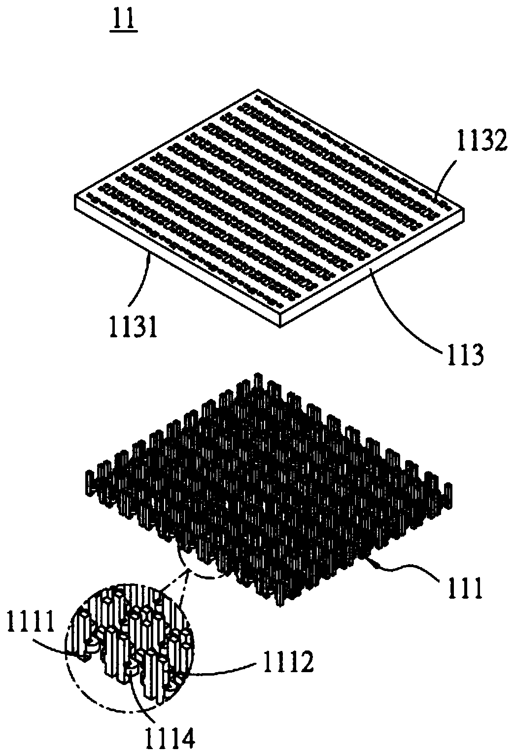
[0057] This embodiment provides a method for manufacturing a chip package structure semi-finished product, a chip package structure module, and a chip package structure. For the description o...


PUM


Abstract

The invention provides a chip package structure semi-finished product, a module, and a fabrication method of a chip package structure semi-finished product. According to the invention, a plurality ofconductive terminals are positioned by a positioning shell to be synchronously arranged, so that the arrangement time of the conductive terminals is reduced, and then, the positioning shell is removedto expose the top lap joint parts of the conductive terminals to be electrically connected with a preset circuit substrate or an electronic assembly. The chip package structure module can quickly form a plurality of chip package structures in a cutting mode, so that the manufacturing process of the chip package structures is simplified, and the yield of products is increased.

Description

technical field [0001] The invention relates to an integrated circuit packaging process, in particular to a chip packaging structure semi-finished product, a chip packaging structure module and a manufacturing method of the chip packaging structure. Background technique [0002] In the traditional IC packaging process, the number of conductive terminals is large, which makes the layout of the conductive terminals very cumbersome. It is often necessary to deploy a machine to send each conductive terminal to the circuit substrate one by one for welding, resulting in a long time for the layout of the conductive terminals and lowering the manufacturing cost. stay high. [0003] Therefore, in the IC packaging process, how to reduce the difficulty of laying the conductive terminals and solve the problem of long laying time of the conductive terminals has become a technical issue that the industry is eager to challenge and overcome. Contents of the invention [0004] In view of ...

Claims


Application Information

Patent Timeline
Patent Type & Authority Applications(China)
IPC IPC(8): H01L23/48H01L23/31H01L21/50
CPCH01L21/50H01L23/3107H01L23/48
Inventor 黄睦容陈盈仲
Owner TARNG YU ENTERPRISE
Why Eureka
Try Eureka