Composition, OLED device, OLED display panel and display device

A display panel and display device technology, which is applied in the manufacture of semiconductor devices, electrical solid state devices, semiconductor/solid state devices, etc., can solve the problems of carrier balance destruction, electron and hole mobility increase, etc., so as to improve the balance, Effect of reducing drive voltage rise and reducing dependence

Inactive Publication Date: 2020-03-24
KUNSHAN GO VISIONOX OPTO ELECTRONICS CO LTD
View PDF5 Cites 1 Cited by
  • Summary
  • Abstract
  • Description
  • Claims
  • Application Information

AI Technical Summary

Problems solved by technology

Under the irradiation of sunlight, the temperature of the OLED device will increase, resulting in the increase of the mobility of electrons and holes in the OLED device, and the ratio o

Method used


Image

  • Composition, OLED device, OLED display panel and display device
  • Composition, OLED device, OLED display panel and display device
  • Composition, OLED device, OLED display panel and display device

Examples


Embodiment 1

[0038] This embodiment provides a composition for the electron transport layer of an OLED device. The composition includes 1% to 99% of a partial electron transport type low-mobility metal complex material and 1% to 99% Organic electron-transporting materials, wherein the electron mobility of the partial electron-transporting low-mobility metal complex material is less than 1*E -7 cm 2 / Vs.

[0039] Specifically, in this embodiment, a partial electron transport type low-mobility metal complex material is incorporated into an organic electron transport material, and the electron mobility of the partial electron transport type low-mobility metal complex material is less than 1*E -7 cm2 / Vs, compared with a single organic electron transport material, the electron mobility of the composition of this embodiment is better. In addition, after the partial electron transport type low-mobility metal complex material is mixed into the organic electron transport material, compared with ...

Embodiment 2

[0068] As mentioned in the background technology, OLED devices in the prior art have the problem of aging too quickly under high-temperature environment. The inventors found that the main reason is that the existing OLED devices are unbalanced in the high-temperature environment. Further research by the inventors found that , the reason why the current OLED device downloads carriers in a high-temperature environment is unbalanced, mainly because the mobility of both electrons and holes in the OLED device will increase in a high-temperature environment, and the ratio of the increase in the mobility of electrons and holes is different.

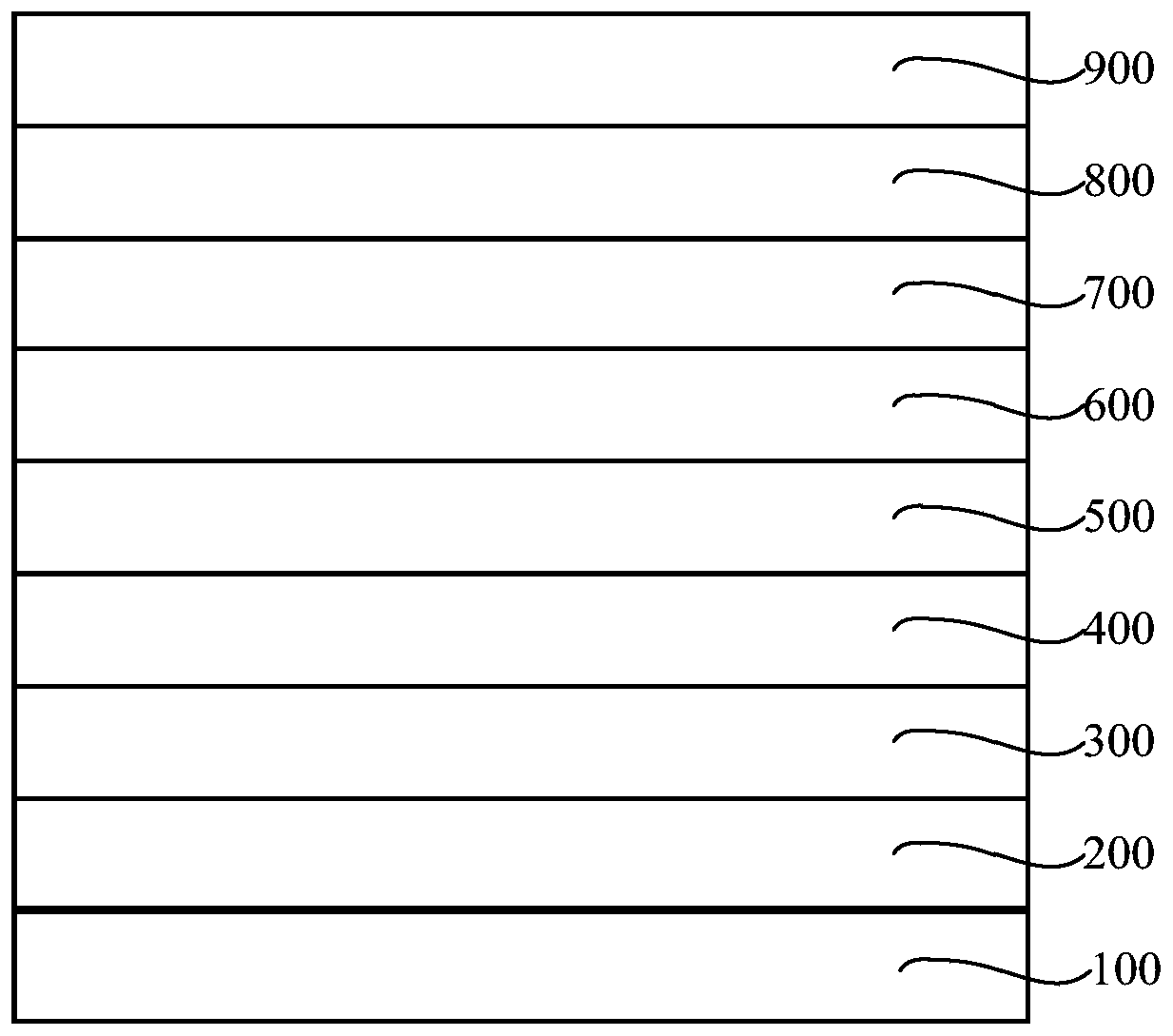
[0069] figure 1 A schematic structural diagram of an OLED device provided for an embodiment of the present invention; please refer to figure 1 . In view of the above problems, this embodiment provides an OLED device, including an anode layer 100, a cathode layer 900, and a hole injection layer 200, a hole transport layer 300, and an electron bl...

Embodiment 3

[0100] This embodiment provides an OLED display panel, and the OLED display panel includes the OLED device described in the second embodiment above.

[0101] The OLED display panel of this embodiment adopts the above-mentioned OLED device, so the electron mobility in the electron transport layer is less affected by the electric field and temperature, the balance of the carrier system in a high temperature environment is better, and the life span at a high temperature is longer. high.


PUM


Abstract

The invention provides a composition, an OLED device, an OLED display panel and a display device. The composition comprises 1%-99% of a partial electron transport type low-mobility metal complex material and 1%-99% of an organic electron transport material, and the electron mobility of the partial electron transport type low-mobility metal complex material is smaller than 1 * E-7cm < 2 >/Vs. According to the invention, the influence of an electric field and temperature on the electron mobility in the electron transport layer can be reduced, the balance of a carrier system in a high-temperatureenvironment is good, and the service life at a high temperature is long.

Description

technical field [0001] The invention relates to the field of display technology, in particular to a composition, an OLED device, an OLED display panel and a display device. Background technique [0002] Organic Light Emitting Diode (OLED) devices have attracted widespread attention because of their advantages such as self-illumination, rich colors, fast response, wide viewing angle, light weight, thin thickness, low power consumption, and flexible display. . Moreover, OLED display devices made of OLED devices are regarded as display devices with great application prospects, especially in the field of flat panel display, OLED display devices are considered to be a trend. At present, OLED display devices have been widely used in fields such as mobile phones, watches, televisions, computers, and vehicle display screens. [0003] In some special application scenarios (such as vehicle display screens), OLED display devices may be exposed to sunlight for a longer period of time ...

Claims


Application Information

Patent Timeline
IPC IPC(8): H01L51/50H01L51/54H01L27/32
CPCH10K59/00H10K85/30H10K50/165H10K50/16H10K85/654H10K85/6565H10K85/324H10K85/6572
Inventor 王虎赵伟李梦真许瑾曹方义刘彬周小康
Owner KUNSHAN GO VISIONOX OPTO ELECTRONICS CO LTD
Why Eureka
Try Eureka