
A kind of insulating and heat-conducting material for semiconductor and preparation method thereof

A technology of insulation and heat conduction, heat conduction and insulation fillers, applied in the direction of heat exchange materials, insulators, organic insulators, etc., can solve the problems of difficulty in ensuring the insulation of composite materials, damage to the insulation performance of composite materials, and difficulty in application, etc., to achieve high thermal conductivity, Improve heat dissipation efficiency and good thermal stability

Active Publication Date: 2021-10-26
SOUTH UNIVERSITY OF SCIENCE AND TECHNOLOGY OF CHINA
View PDF8 Cites 0 Cited by
  • Summary
  • Abstract
  • Description
  • Claims
  • Application Information

AI Technical Summary

Problems solved by technology

In particular, the unique two-dimensional structure of graphene shows an ultra-high thermal conductivity. The invention patent application number 201310093737.8 discloses a high thermal conductivity insulating polymer composite material. The thermal conductivity filler contains graphene, but since graphene is an electrical conductor , has fatal damage to the insulation performance of the composite material. When the semiconductor device generates heat and the temperature rises when it is in operation, it is affected by the high temperature, and the thermal conduction path of the composite material may evolve into a conductive path, and the insulation of the composite material is more difficult to guarantee. It is difficult to apply in the insulation and heat dissipation occasions that require high insulation performance

Method used


Image

  • A kind of insulating and heat-conducting material for semiconductor and preparation method thereof

Examples


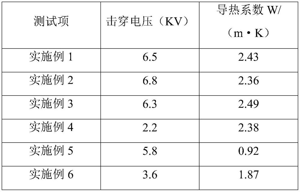
Embodiment 1

[0021] According to the weight of the weight, 60 parts of the thermoplastic resin, 10 parts of dispersing agent, 15 parts of adhesive, 9 expanded graphite and 12 bubble powder were prepared, and the semiconductor was prepared in the following method:

[0022] (1) In the adhesive, the expanded graphite and the sea bubble powder are added to the adhesive, and the mixture is mixed after mixing.

[0023] (2) The thermoplastic resin and dispersing agent, the curing agent are added to the mixture obtained from step (1), and the insulative thermally conductive material for the semiconductor is obtained at 100 to 160 ° C.

[0024] Among them, the thermoplastic resin is polymethyl methacrylate, the dispersant is polyvinylpyrrolidone, and the adhesive is a polystyrene adhesive and acetate adhesive, polystyrene adhesive and ethyl acetate. The mass ratio of the adhesive is 2: 5.

Embodiment 2

[0026] According to the weight of the weight, 50 parts of the thermoplastic resin, 7 parts dispersants, 10 parts of adhesives, 6 expanded graphite and 8 seafubi powder were prepared, and the semiconductor was prepared in the following method:

[0027] (1) In the adhesive, the expanded graphite and the sea bubble powder are added to the adhesive, and the mixture is mixed after mixing.

[0028] (2) The thermoplastic resin and dispersing agent, the curing agent are added to the mixture obtained from step (1), and the insulative thermally conductive material for the semiconductor is obtained at 100 to 160 ° C.

[0029] Among them, the thermoplastic resin is a polyamide, the dispersant is polyoxyethylene ether methacrylate, and the adhesive is a polystyrene adhesive and acetate adhesive, polystyrene adhesive and acetate The mass ratio of the ester adhesive is 1: 3.

Embodiment 3

[0031] According to the weight of the weight, 70 thermoplastic resins, 13 parts dispersants, 20 partial adhesives, 13 expanded graphite and 15 semibubic powder were prepared, and the semiconductor was prepared as described below:

[0032] (1) In the adhesive, the expanded graphite and the sea bubble powder are added to the adhesive, and the mixture is mixed after mixing.

[0033] (2) The thermoplastic resin and dispersant are added to the mixture obtained from step (1), and the curing agent is added to obtain a semiconductor insulated thermally conductive material in 100 to 160 ° C.

[0034] Among them, the thermoplastic resin is polyphenylene ether, the dispersant as polyoxyethylene ether acrylate, adhesive is a polystyrene adhesive and acetate adhesive, polystyrene adhesive and acetic acid The mass ratio of ethyl adhesive is 1: 2.


PUM


Abstract

The invention belongs to the field of insulating and heat-conducting materials, and discloses an insulating and heat-conducting material for semiconductors and a preparation method thereof. In parts by weight, the insulating and heat-conducting material for semiconductors comprises 50-70 parts of thermoplastic resin, 7-13 parts of dispersant, 5-10 parts of curing agent, 10-20 parts of adhesive, 6-13 parts of expanded graphite and 8‑15 parts meerschaum powder. The expanded graphite in the present invention has a rich pore structure, high thermal conductivity, and good thermal stability. When used in combination with sepiolite powder and thermoplastic resin, the obtained composite material can not only solve the problem of heat accumulation in electronic device modules, but also improve its performance. High heat dissipation efficiency and good electrical insulation.

Description

Technical field [0001] The present invention relates to the field of insulating thermally conductive materials, and in particular to a semiconductor insulating thermally conductive material and a preparation method thereof. Background technique [0002] The LED is a semiconductor light emitting diode built on a semiconductor transistor. With the continuous improvement of semiconductor technology and manufacturing process, the light flux and lighting efficiency of LEDs have been continuously improved, and the power LED has been widely used in daily life and industrial production. However, as the LEDs develop toward high light strength, high power direction, its heat dissipation problem has been highlighted. [0003] In addition to the LEDs, electronics, especially high-power, and there will be a lot of heat generation during the operation of miniature electronic components. If heat dissipation is not time, the amount of heat accumulated too much will affect the normal operation of...

Claims


Application Information

Patent Timeline
Patent Type & Authority Patents(China)
IPC IPC(8): C08L33/12C08L39/06C08L25/06C08L31/04C08K9/00C08K3/04C08K7/26C08L77/00C08L71/02C08L71/12C09K5/14H01B3/44H01B3/30H01B3/42
CPCC08L33/12C08L71/12C08L77/00C08L2203/20C08L2205/035C09K5/14H01B3/305H01B3/427H01B3/447C08L39/06C08L25/06C08L31/04C08K9/00C08K3/04C08K7/26C08L71/02
Inventor 曲作鹏叶怀宇田欣利张国旗
Owner SOUTH UNIVERSITY OF SCIENCE AND TECHNOLOGY OF CHINA
Learn More